What is Cascading of Amplifier Stages?
A single stage of amplifier can provide only a limited current gain or voltage gain. Most of the applications require much higher gain. Hence, we usually use several amplifier stages connected in cascade i.e. connected such that the output of one stage becomes the input to the next stage. Thus, a multistage amplifier or cascade amplifier may provide a higher voltage gain or current gain.
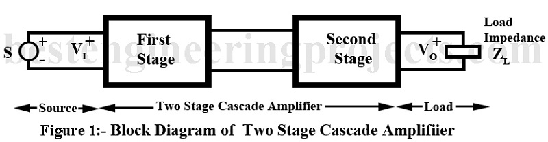
Cascading of amplifier stages is usually done to increase the total gain of the amplifier. However, sometimes cascading is done to get the desired output and input impedance for specific applications. Figure 1 gives the block diagram of two-stage amplifier. The first stage is driven by a voltage source Vs having series source resistance Rs. Alternatively, the driving source may be current source Is with shunt resistance Rs. the output of the first stage is fed to the input of the second stage while the output of the second stage feeds the load impedance ZL.
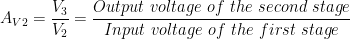
Actual voltage available at the input of the first stage is Vi while V0 is the output voltage of the second stage. Then the ratio  forms the voltage gain of the two stage cascade amplifier. Instead of two stages as shown in figure 3, we may have three or more stages connected in cascade amplifier, it becomes possible to amplify a weak input voltage Vi of just a few microvolts to get an output voltage V0 of several volts.
Cascading of Amplifier Stage using Transistor
Transistor amplifier may be connected in any of the three configurations namely common emitter (CE), common base (CB) and common collector (CC). However, in cascade amplifier meant for providing high gain, only CE amplifier stage are connected in cascade. CB and CC configurations can not be used for this purpose.
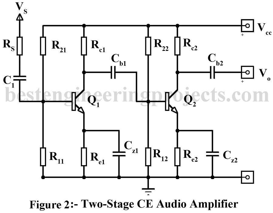
Figure 2 gives the circuit of a two stage CE audio amplifier. The circuit gives the typical biasing arrangement and use of coupling capacitors Cb1 and Cb2. Typical values of circuit components are also given. The load impedance is a resistor while coupling is through a capacitor. Hence this cascade amplifier forms the so-called resistance – Capacitance coupled or RC coupled amplifier. Other circuit arrangement is also popular for specific uses. However, we here take up R.C. coupled amplifier since this is the one most popularly used for audio frequency amplification. Circuit of figure 2 is given here just to give an impression as to what a typical 2-stage CE audio amplifier looks like.
Analysis | Cascading of Amplifier Stages
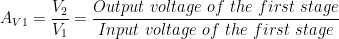
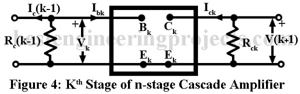
For the purpose of analysis we take up a general n-stage CE cascade amplifier. Figure 3 gives the block diagram of the same giving the various voltages, currents and resistances involved. In Figure 3, the biasing arrangement and coupling elements have not been shown for the sake of celerity. We now proceed to derive expressions for voltage gain, current gain, power gain, input impedance and output impedance of this amplifier.
(A) Voltage Gain:
The voltage gain of the complete cascade amplifier is simply the product of the voltage gains of the individual stage. This is proved below.
Voltage gain of first stage is,
 …..(1)
Where AV1 is the magnitude of the voltage gain and  is the phase angle of the output voltage V2 relative to the input voltage V1. The output voltage V2 of the first stage forms the input voltage of the second stage. Hence
Voltage gain of second stage is,
 ……(2)
……(2)
Similar expressions may be written for the remaining stages.
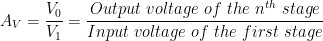
Then the voltage gain of the complete n-stage cascade amplifier is given by,
 …..(3)
Where Av is the magnitude of the voltage gain and  is the phase angle of the output voltage V0 relative to the input voltage V1
But  ……(4)
……(4)
From equation 4 we conclude that
 ……(5)
……(5)
Or 
 …..(6)
Hence  ……(7)
……(7)
And  ……(8)
……(8)
From Equation (7) we conclude that the magnitude of voltage gain of the complete cascade amplifier is equal to the product of the magnitude of voltage gains of the individual stages.
From Equations 8 we conclude that the phase shift of the voltage gain of the complete cascade amplifier is equal to the sum of the phase shift of the individual stages.
Calculation of the Voltage Gain Avk of Kth stage:
Figure 4 shows one intermediate stage, say kth stage, of n-stage cascade amplifier.
Then the voltage gain of this kth stage is given by,
 …..(9)
Where Rik is the effective load impedance at the collector of the kth stage.
Quantities AIK, RLK and Rik may be evaluated on starting from the last stage i.e. nth stage and processing backward. Thus, for the nth stage, current gain ALn and input resistance Rin are given by,
 ……..(10)
And,
 ….(11)
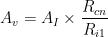
Where RLn is the effective load impedance of the last stage and is equal to Ren.
For the (n-1)th stage, effective load impedance Ri(n-1) is equal to Rc(n-1) || Rin. Thus,
 …..(12)
Next we calculate the current gain AI(n-1) of the (n-1)th stage using Equation 10 on replacing RLn by RL(n-1). Similarly, we calculate the input impedance Ri(n-1) of the (n-1)th stage from Equation 9 no replacing AIn by AI(n-1) and RLn by RL(n-1). Thus, we procced backward to calculate the current gain and input impedance of each stage from nth to the first. Then the voltage gain of each stage may be calculated using Equation 8 relevant to the stage.
Voltage gain of the complete cascade amplifier may then be calculated using Equation 5.
Calculation of Current Gain AI of Kth Stage
 …..(13)
Now  ……(14)
Or,  …..(15)
Where AI1 is the base-to-collector current gain of the first stage and equals  while A’I2, A’I3 etc. are the collector-to-collector current gains of second, third etc. stages.
For kth stage, collector-to-collector current gain A’IK is given by
 …..(16)
Similarly, base-to-collector current gain AIK is given by
 …..(17)
Relation between A’IK and AIK
From Figure 4,
 …..(18)
Where Rik is the input impedance of the kth stage.
Hence  …..(19)
Value of A’IK as given by Equation 19 may be substituted in equation 15 to give the resultant current gain AI.
Steps involved in Evaluating Current gain AI
- Find the base-to-collector current gain AIn for the nth or the last stage making use of equation 10.
- Find the input impedance of the last stage making use of Equations 11.
- Calculate the effective load resistance RL(n-1) for the (n-1)th stage using Equation 12
- Repeat steps 1 to 3 for (n-1)th, (n-1)th stage to find the AIK for the kth stage.
- Find the collector-to-collector gain A’IK for the kth stage using equation 19.
- Find the resultant current gain AI for the complete n-stage cascade amplifier using Equation 15.
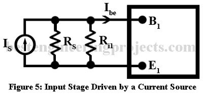
Overall Current Gain Considering the source Resistance:
Let the input stage of the n-stage cascade amplifier be driven from a current source Is as shown figure 5. Then the overall current gain of the cascade amplifier is given by,
 …..(20)
Alternative Method of Calculating AI | Cascading of Amplifier Stages
Alternative we may calculate AI making use of the following relation:
 …….(21)
Where Av is the voltage gain of the complete cascade amplifier.
 …..(22)
Alternative using Equation 21, we get, 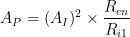 …..(23)
Input Impedance | Cascading of Amplifier Stages
The input impedance of the complete cascade amplifier may be found following the same procedure as for calculating the voltage gain. Thus, we start from the last stage and proceed backward. The steps involved are as below:
- Calculate base-to-collector current gain AIn for the last stage using Equation 10.
- Calculate input impedance Rin of the last stage using Equation 11.
- Calculate effective load impedance
 for the (n-1)th stage using Equations 12.
 - Calculate and for the (n-1)th stage and for the (n-2)th
- Proceed in this manner and finally calculate the input impedance of the first stage.
 for the (n-1)th stage using Equations 12.
 and
and  for the (n-2)th
Output Impedance | Cascading of Amplifier Stages
For calculating the output impedance of each stage and that of the complete cascade amplifier, we proceed forward starting from the first stage. The output admittance of the first stage is given by,
 …..(24)
Then  gives the corresponding output impedance R01.
The output terminal impedance Rot1 of the first stage is equal to the parallel combination of R01 and Roc1.
Thus  …..(25)
This Rot1 forms the source impedance for the second stage. Equation 24 may now be used again to find Y02 of the second stage using R0t1 in place of Rs. The output terminal impedance Rot2 of the second stage is parallel combination of  and RC2.
We may proceed in this manner to find the output impedance of the third, fourth etc. stage and finally the last stage. In the above derivation we have assumed CE configuration. However, the method given above for calculating AV, AI, Ri and R0 is general in nature and may also be used for CB and CC configurations.
Choice of Transistor Configuration in a Multistage Amplifier
Choice of transistor configuration to be used for intermediate stages in a multistage amplifier depends on the maximum voltage gain provided by the configuration. hence CC configuration can not be used since a stage of CC amplifier gives voltage gain less than unity. A single stage CB amplifier, no doubt, gives voltage gain more than unity but intermediate stage can not use even CB configuration since the overall voltage gain of multistage amplifier using VB configuration is low, almost equal to the voltage gain of the last stage alone. This becomes evident from the following discussion.
The voltage gain AVk of any stage, say Kth stage is given by,
 ……(26)
But,  …..(27)
Hence, 
Assuming the stage to be identical i.e. assuming that Ri(k+1) = Rik, we conclude that RLK < Rik. Further the maximum value of current gain AIK in CB configuration in hfb which is slightly less than unity. Hence as per Equation 26, AVk for any CB stage except the last stage is less than unity. Hence we conclude that even CB configuration is not suitable for use in intermediate stages.
CE stage are popularly used for intermediate stages since hfe for a CE stage is much greater than unity.
Input Stage | Cascading of Amplifier Stages
For input stage, the consideration is not the maximum voltage gain but the impedance matching of the source with the input impedance of the input stage. Some driving sources may require input circuit to be an almost open circuit while others need an almost short circuit. Hence we may be required to use CC or CB configuration for the input stage for proper impedance match at the cost of voltage or current gain. In certain other cases, choice of configuration for the input stage is the minimization of noise and maximization of single/noise power ratio.