Common Collector Amplifier or the Emitter Follower: Figure 1(a) gives the basic circuit of a common collector amplifier, popularly called emitter follower. Its voltage gain is close to unity (one) and, therefore, any increment in the input voltage i.e. the base voltage appears as an equal increment in the output voltage across the load resistor in the emitter circuit.
Thus, the emitter may be said to follow the input signal and hence the name emitter follower. The input resistance Ri of a CC amplifier or emitter follower is very high, of the order of hundred of kilo-ohms while its output resistance is very low, of the order of tens of ohms. High Ri and low R0 permits us to use emitter follower as an impedance matching stage to match the high output impedance of one amplifier stage to the low input impedance of the next stage over a wide frequency range. With voltage gain very close to but slightly less than unity, the emitter follower serves the function of resistance transformation. Further emitter follower increases the power level of the signal since its current gain AI is quite large.
Analysis of Common Collector Amplifier or the Emitter Follower
Figure 1(b) gives the small signal equivalent circuit of the emitter follower of figure 1(a) on
- Omitting dc voltage source
- Omitting the biasing resistor R1 – R2 and the coupling capacitor CC and
- Replacing the transistor by its small signal two generator h-parameter model.
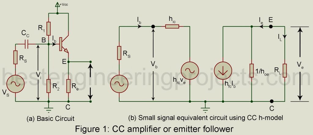
Here also we assume sinusoidal input signal. Hence in the equivalent circuit, we have used rms values of voltages and currents nearly Ib, Vb, Ie, Ve.
The equivalent circuit of figure 1(a) is similar to that of CE amplifier of Figure 2. Hence the analysis procedure is exactly the same. The expression of AI, Ri, AV, AIS, AVS and Y0 are, therefore, the same as of CE amplifier except that h-parameters of CC configuration are used. We may make use of Table 1 and simultaneously use conversion Table 2 to get the expression for AI, Ri, AV and R0.
Table 1: Result of small single analysis of low frequency cc amplifier |
|
 |
 |
 |
 |
 |
 |
Table 2 Approximate Conversion Formulas for h-parameter |
|
 |
 |
 |
 |
 |
 |
 |
 |
Thus, from Table 1 and Table 2,
Current gain  …..(1)
Input resistance 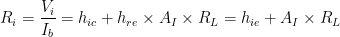 …..(2)
Voltage gain 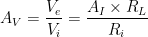 …..(3)
But from equation (2) 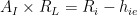
Hence  …..(4)
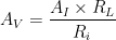
Overall voltage gain  …..(5)
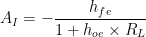
Overall current gain  …..(6)
Output admittance  ……(7)
……(7)
Power gain 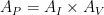 …..(8)
Example 1 A transistor amplifier in CC configuration is driven by a voltage source Vs of internal resistance Rs = 1000 . The load impedance is a resistor RL = 4000
 . The h-parameters are:
  , hfc = -51 and
  . Calculate for this amplifier, the current gain AI, input resistance Ri, voltage AV, overall voltage gain AVS, overall current gain AIS, output resistance R0 and power gain AP.
Solution:
Current gain 
Input Resistance 
Voltage gain 
Overall Voltage gain 
Overall current gain 
Output admittance 
Output resistance 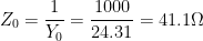
Power gain 