A pulse generator circuit cum timer circuit is a multipurpose instrument. In the case of the electronics field, it is that apparatus without which the design of the project becomes a complicated task. Multiple types of such circuits might have been available in the market. But the circuit we are going to discuss here overshadows them with the range of features it offers variable frequency, variable pulse width, and variable amplitude. To add more to it, we can use this instrument like a timer too in case of need. It can also be included in direct relay operation since it offers high voltage (up to 24V).
The pulse generator circuit grants a wide frequency response of 0.001 Hz to 5 MHz, and a wide variation of pulse width: 100 nanoseconds to 10 seconds. And, the main point is it is reasonably accurate. Similarly, it also gives true positive/negative pulses (+24V or -24V) and has a separate output arrangement for TTL gates (4.35V). These outputs thus arranged are so arranged that they are protected from short circuit conditions.
Circuit Description of Pulse Generator Circuit Cum Timer Circuit
The major component of the project ‘Pulse Generator circuit cum Timer circuit’ is 7404 TTL hex inverter IC which is used as an astable multivibrator. This IC can be used to get up to 18 MHz but it is operated to give up to 5 MHz only.
Components like R1, C1, and VC1 are used to set the frequency of the generator. Among them, R1 and C1 are fixed and VC1 is an air dielectric gang condenser whose value is variable up to 500 pF. This condenser is provided with two separate terminals and one common terminal. Out of which the two separate terminals are shorted. The terminals are shorted and the other common terminal is connected across C1. And, by adjusting or rotating gang condenser VC1, we can obtain the output frequency varying from 5 MHz to 1 MHz as required.
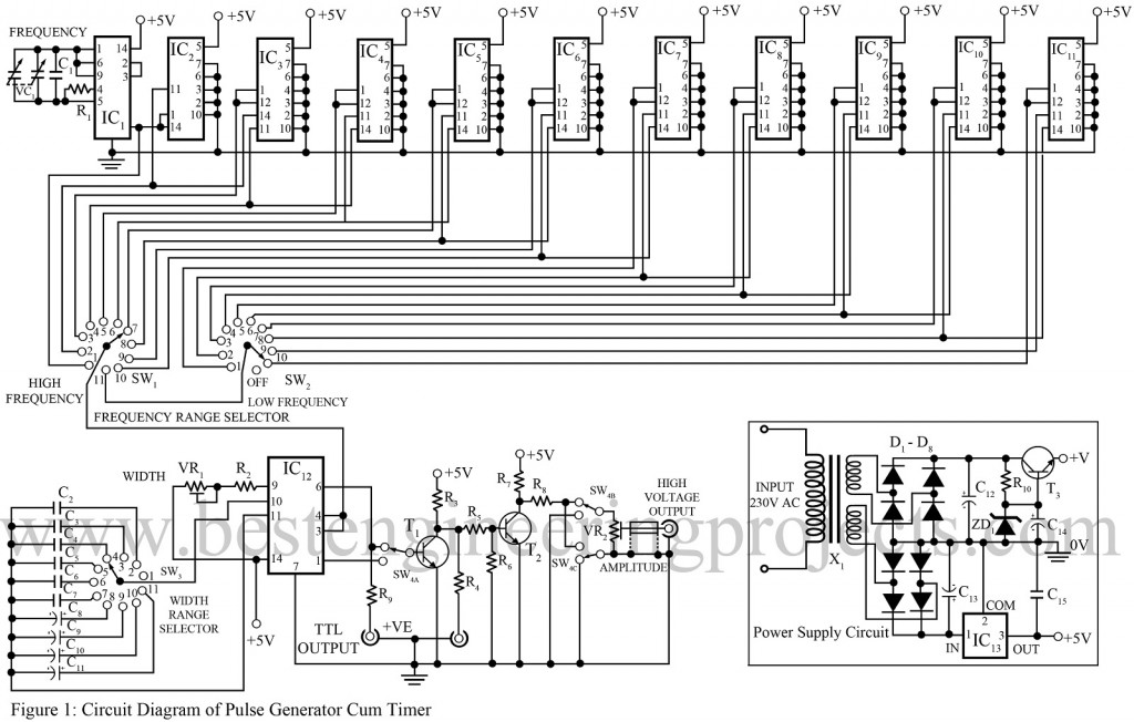
The output thus obtained is supplied to multiple ICs to produce a wide range of frequencies. Firstly, it is fed to IC2, a 7490 TTI frequency divider which is functioning as a divider-by-five in the circuit. This is then followed by IC3 which is another 7490, used as a divider-by-two. The output of IC3 is further divided by C4 acting as a divider-by-five. This alternate division by two and by five is repeated by IC5 through IC11. All these ICs are connected in cascade and to a band-switch like IC3 and IC4.
This arrangement thus designed ensures the selection of a wide range among 5MHz to 1 MHz, 1 MHz to 500kHz, 500kHz to 100kHz, 100kHz to 50kHz, 50kHz to 10kHz, 10kHz to 5kHz, 5 kHz to 1 kHz, 1 kHz to 500Hz, 500Hz to 100Hz and 100Hz to 50Hz through band-switch SW1 as shown in the figure. In the same way, band-switch SW 2 enables the selection of a low-frequency range from 50Hz to 10Hz, 10Hz to 5Hz, 5 Hz to 1Hz, 1Hz to 0.5Hz, 0.5Hz to 0.1Hz, 0.1Hz to 0.05Hz, 0.05Hz to 0.01Hz, 0.01Hz to 0.005Hz and 0.005Hz to 0.001 Hz which is followed by “off” position.
This arrangement is then followed by IC12 which also operates as a monostable multivibrator. It is a 74121 TTL IC that can control the width of a pulse from 40 nano-sec to 28 sec. The range selection switch selects a timing condenser among C2 to C11 and a continuous variable is obtained through VR1.
To get a fixed output voltage(4.3V) at the TTL output, the output of monostable IC12 is given through switch SW4A to high-speed switching transistor T1 (a 2N2369A). Resistor R4 functions as a limiting resistor to protect the transistor from short circuits. Resistors R8 and R11 also perform similar functions. The output amplitude can be kept at either 12V or 24V. The only changes that have to be made are:
The power supply circuit is simple. IC13 is a 7805 (three-pin 5V regulator IC) and the positive supply is simple Zener regulated. IC13 must be mounted on a large heat sink. It is better to have this IC in the T03 pack for good heat dissipation as under the worst condition the current will be 50*15, i.e. 750 mA.
Construction of Pulse Generator Circuit Cum Timer Circuit
One must take extra care in the construction of this circuit since it is a TTL high-frequency circuit. Getting started with, firstly connect IC13 and other power supply components and make sure you are getting +5V supply concerning the earth. Thereafter, connect IC1, C1, and R1 keeping VC1 unconnected, and then observe the waveform.
Once you obtain a waveform about (3V) then connect VC1 and examine the waveform again. You should get the frequency range of 5MHz to 1MHz. The range may not be precisely the same as stated, however, you can obtain the output around this range or even a slightly wider range of frequency by the full rotation of the gang condenser.
In case you do not get the full range, check on IC1. If that doesn’t work, check C1 and R1, and lastly check VC1. Sometimes, it can be due to the dust particles contained in the air gang condenser or even the plates might be shorting. In that case, clean the dust or carefully separate the plates. And then it should start working. During cleansing, don’t hesitate to clean this gang condenser as well so that you may not face the same difficulty afterward. Now connect IC2 and check the output. Then connect IC3 and check the output again, and repeat the same up to IC11. Do not connect switches SW1 and SW2 yet. Now connect IC12 with SW3, C2 to C11, R2, and VR1. Keep the input wire, i.e. the wire connected to pins 3 and 4 of IC12 to 10KHz, and check on each range of SW3 to ensure that you are getting proper output.
As mentioned in earlier paragraphs, this is a high-frequency circuit, and therefore all wires connected to SW3 (as also to SW1 and SW2) must remain parallel to each other. You can make use of insulation tape to achieve a parallel arrangement. On the other hand, the connections to VR1 and VC1 should be done through a twin lead, like the wire used for a TV antenna.
When you are sure the circuit is operating properly, connect transistors T1 and T2 and the remaining components of the circuit i.e. resistors. The circuit has been divided into two sections only to avoid complexities in case of error prediction in the circuit which is obvious in such projects. Hence do not proceed to the next portion unless you are sure that the preceding circuit functions as required.
Calibration of Pulse Generator Circuit Cum Timer Circuit
For the effective outcome of the project, calibration must be done with a good oscilloscope that has a frequency response of at least up to 10 MHz. Keep SW1 in the first position and SW3 off. Then rotate VC1 and mark on 5MHz, 4MHz, 3MHz, 2MHz, and 1MHz positions. During rotation, one should note that the full rotation of the gang condenser might vary the frequency from 5.8 MHz to 0.6 MHz but do not calibrate the remaining frequencies since these are not useful frequencies in the project we are discussing.
Now keep SW1 in the second position and check if the previous markings coincide with the positions of the gang condenser for 1 MHz, 0.9 MHz, 0.8 MHz, 0.7 MHz, 0.6 MHz, and 0.5 MHz. Following the same pattern, switch SW1 to the other positions to verify the calibration further.
Similarly to verify the calibration of SW2, use LED in series with 220-ohm, 1/4W resistor and connect it to TTL positive output and note the precise time between LED flickering. To calibrate the pulse width, set frequency 5MHz, keep SW3 in the first position, change VR1 and take note of divisions like 50n, 60n, 70n, 80n, 100n sec, etc. Now without changing the set frequency, calibrate each range. Lastly, calibrate the amplitude.
Check out more other timer circuits posted on bestengineeringprojects.com
- Sound Activated 0-30 Minutes Timer Circuit
- Industrial Timer Circuit
- Countdown Timer Using Arduino
- 24 Hour Digital Clock and Timer Circuit
- Digital Clock with Seconds and Alarm Time Display
Some useful hints | Pulse Generator Circuit Cum Timer Circuit
- The gang condenser must be kept in a dust-free plastic box. For better system stability make the full chassis dust-free if possible.
- Use shielded wire for output.
- To drive a relay at a low frequency, use the adapter given in fig.4. It can be kept inside the cabinet, with the rest of the circuit, keeping two output terminals for the relay.
PARTS LIST OF PULSE GENERATOR CIRCUIT CUM TIMER CIRCUIT
| Resistors (all ¼-watt, ± 5% Carbon, Unless Mentioned Otherwise) |
| R1 = 220 Ω, ±1% METAL FILM
R2 = 2 KΩ, ±1% METAL FILM R3, R4, R11 = 100 Ω R5 = 220 Ω R6 = 10 KΩ R7 = See Text R8 = 500 Ω R9 = 1 KΩ R10 = 6.8 KΩ, ½ W VR1 = 47 KΩ, CARBON LINEAR VR2 = 10 KΩ, CARBON LINEAR |
| Capacitors (all good-quality, preferably metalized polyester and tantalum types rated ±10% ). |
| C1, C2 = 1 Pf
C3 = 10 pF C4 = 100 pF C5 = 1000 pF C6 = 0.01 µF C7, C15 = 0.1 µF C8 = 1 µF C9 = 10 µF/6V C10 = 100 µF/6V C11 = 1000 µF/6V C12, C14 = See Test C13 = 1000 µF/16V VC1 = 500 pF, AIR CORE GANG |
| Semiconductors |
| IC1 = TTL 7404, 7405, 74H04 OR 74H05 Hex Inverter
IC2 – IC11 = TTL 7490 Counter Divider IC12 = TTL 74121 One-shot Multivibrator IC13 = 7805, 3-PIN Regulator IC D1 – D8 = 1N4001 Diode ZD1 = See Text T1 = 2N2369A Transistor T2 = See Text T3 = HL100, SL100 or BEL100N |
| Miscellaneous |
| X1 = See Text (230V Primary)
SW1 – SW3 = One-Pole, 11-way Switches SW3 = Three-Pole, two-way Switch Heatsink for IC13 |
| Components | For 12V Output | For 24V Output |
| R7 | 10 KΩ, ¼W | 20 KΩ, ¼W |
| C12 | 500 µF/24V | 500 µF/50V |
| C14 | 100 µF/16V | 100 µF/35V |
| ZD1 | 15V, 400mW | 30V, 400Mw |
| X1 | 0-6V,0-15V, 1A | 0-6V, 0-30V, 1A |
Can I use CD4000 series instead of 74 series i.e CD4017 instead of 74LS90
Can I get a complete writeup on this project?
Please can I get a detailed llayout of this project on PCB