Analysis of Common Emitter Amplifier using H Parameter
Figure 1(a) shows the circuit of a common emitter (CE) amplifier using self-bias and load resistor R0 capacitively coupled to the collector. Figure 1(b) gives the a.c. equivalent circuit. Here we have eliminated the biasing circuit consisting of R1, R2, Re, and Cz.
The R1 – R2 combination is equivalent to resistance Rb (= R1 || R2) between base and ground. It is assumed that Rb is large in comparison with the input resistance of the amplifier between base and ground and hence Rb is neglected in the equivalent circuit. Similarly, the reactance of capacitor Cz is so small at the lowest operating frequency that Cz effectively bypasses all a.c. components.
Hence Re-Cz combination is also excluded from the a.c. equivalent circuit. In most of the amplifiers, the a.c. output voltage developed across Rc is capacitively coupled to the next stage through the capacitor Cb and R0 is the effective impedance in the output circuit. The value of capacitor Cb is chosen so large that its reactance at the operating frequency is small and may be neglected. Then for a.c. the operation, R0 comes in parallel with Rc, and effective load resistance RL = RC || RO. This results in the simple a.c. equivalent circuit of Figure 1(b).

Analysis of Common Emitter Amplifier using H Parameter:
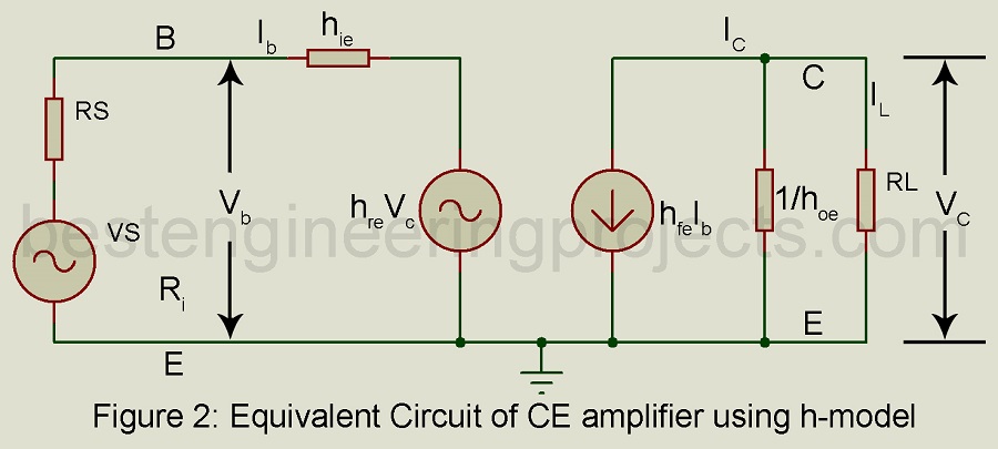
For analysis, we replace the transistor with its small-signal two generator h-parameter model. This results in the equivalent circuit of Figure 2. We assume sinusoidal input. Hence in the equivalent circuit of Figure 2, we have used the RMS value of voltages and currents namely Ib, Vb, Ic, and Vc.
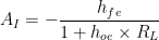
Current Gain or Current Amplification:
Current gain is defined as the ratio of the load current I1 to the input current Ib. Thus,
Current Gain 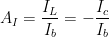 …..(1)
But from figure 2,  …..(2)
Also  …..(3)
Combining Equation (2) and (3) we get,

Hence current gain  …..(4)
Input Impedance Ri:
This is the impedance between the input terminals B and E looking into the amplifier as shown in Figure 2 and is, therefore, given by,
 ……(5)
……(5)
From figure 2  …..(6)
But  …..(7)
Substituting the value of Vc from Equation (7) into Equation (6) we get,
 …..(8)
Hence input impedance  …..(9)
 …..(10)
Where 
From Equation (10) we find that the input impedance Ri is also a function of load resistance RL.
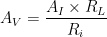
Voltage Gain or Voltage Amplification | Analysis of Common Emitter Amplifier using H Parameter:
It is the ratio of the output voltage Vc to the input voltage Vb. Thus,
Voltage Gain  …..(11)
Output Admittance Y0:
It is the ratio of the output current Ic to the output voltage Vc with Vs = 0. Hence
 with VS = 0 ……(12)
On substituting the value of Ic from Equation (2) into Equation (12) we get,
 …..(13)
But with Vs = 0, Figure 2 gives (Rs + hie) Ib + hre Vc = 0
Or  ……(14)
Combining Equation (13) and (14) we get, 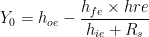 ……(15)
Equation (15) shows that the output admittance Y0 is a function of source resistance Rs. If the source impedance is purely resistive, then the output impedance Y0 is real i.e. purely conductive.
Output impedance  …..(16)
In the calculation of Y0, RL has been considered external to the amplifier. If we include RL in parallel with R0, we get the output terminal impedance Zt given by,
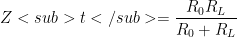 …..(17)
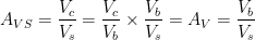
Overall Voltage Gain Considering Rs:
Source voltage Vs applied at the input of an amplifier results in voltage Vb between bae and emitter terminals (input terminals) of the transistor and voltage Vc at the output. Then the overall voltage gain considering the source resistance is given by
 ……(18)
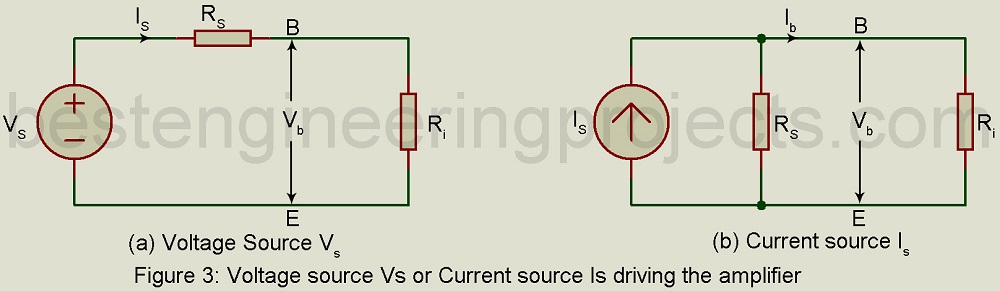
Figure 3(a) given the driven voltage source Vs with source resistance Rs in series. This form of an equivalent circuit for the energy source is known as Thevenin’s equivalent source. This energy source then drives the amplifier represented by its input resistance Ri.
Then  ……(19)
Hence overall voltage gain 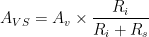 …..(20)
If Rs = 0, then AVS = AV. Thus, AV forms a special care of AVS with Rs = 0.
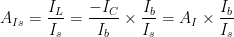
Overall Current Gain Considering Rs:
We may replace the voltage source Vs with series source resistance Rs by what is known as Norton’s equivalent source shown in Figure 3(b), consisting of current source Is with source resistance Rs in the shunt. This current source drives the amplifier resulting in Ib at the input terminals of the amplifier and current IL through the load impedance. Then the overall current gain AIs is given by:
 …..(21)
From Figure 3(b),  …..(22)
Hence overall current gain 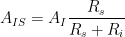 …..(23)
From Equations (20) and Equation (23) we get, 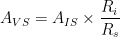 …..(24)
Equation (24) is true provided that the voltage source Vs and the current source Is have the same source resistance Rs.
Power Gain Ap:
From the circuit of Figure 2, the average power delivered to the load imprudence RL is given by:
 ……..(25)
Where  is the phase angle between VC and IL. ……(26)
If load impedance is purely resistive, then cos  and Equation (26) reduce to:
 …..(27)
The input power at input port is,  …..(28)
The power gain AP is the ratio of power PL delivered to the load to the input power at the input port. Thus,
 …..(29)
Table 1 gives the above derivations in tabular form. The expression for AV, AVS, and AIS do not involve h-parameters, while the expression for AI, Ri, and Y0 involves the h-parameters. These expressions may be used for CB and CC configurations and also, of course, for using corresponding h-parameters.
Table 1: Result of small single analysis of low frequency ce amplifier |
|
 |
 |
 |
 |
 |
 |