The Operating Point of Common Emitter Amplifier
From the study of transistor characteristics, we find that amplification by transistor amplifier is most linear when the transistor operates in its active region. Hence the operating point must be suitably placed in the middle of the active region by suitable selection of external energy associated biasing circuit.
Circuit Description of Common Emitter (CE) Amplifier
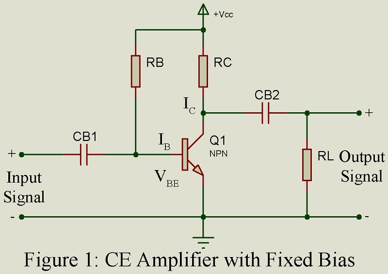
Figure 1 gives the basic circuit of CE amplifier using NPN transistor bias through use of resistor Rb. Here capacitor Cb1, acts as the coupling capacitor to couple the input signal to the base-to-emitter terminals of the transistor. One end of the input voltage Vi is at the ground potential. Vcc is the collector supply voltage which serves the additional function of providing the bias current IB. Under zero signal condition, Cb1 acts as an open circuit since the reactance of a capacitor is infinity at zero frequency (dc).
Thus, the capacitor Cbl acts as blocking capacitor. Normally Cb1 is chosen so large that at the lowest signal frequency, its reactance is small enough to be considered as a short circuit. Thus, capacitor Cb1 blocks dc voltage but passes a.c. signal voltage. Similarly, capacitor Cb2 serves the same two functions. Thus, Cb2 works as coupling capacitor and feeds the amplified a.c. signal to constitute the output voltage V0 across RL. Simultaneously Cb2 blocks the d.c. voltage. Thus, the amplified output a.c. voltage may be applied to the input of the next amplifier stage without affecting the bias of the next stage.
DC and AC Load Lines | Common Emitter (CE) Amplifier
For given collector characteristics and transistor biasing, selection of proper operating point involves selection of suitable values of Rc and Vcc.
Collector current Ic is a function of VCE and base bias current IB and may be put mathematically as,
 …..(1)
Equation 1 represents the static output characteristic of the CE transistor for base current IB.
On applying Kirchhoff’s voltage law (KVL) to the collector circuit including only RC. (excluding Cb2 and RL) We get,
 …..(2)
Equation 2 represents a straight line having intercept Vcc on the voltage axis and intercept  on the current axis. The slope of this line equals
  . This line is referred to as the load line and represents the dynamic characteristic of the device. The zero-signal operating point must be suitably located on this load line. This, in turn, depends on the value If RL. If
  , RL can be neglected and then for large symmetrical input signal (base current in this case), the operating point P1 should be located in the centre of the dc load line. Vc and Ic are the zero-signal collector voltage and collector current respectively at the operating point. Next on application of a time varying signal, base current varies symmetrically on either side of IB1, the point of operating moves along dc load line symmetrically about the zero-signal operating point P1 and the instantaneous collector voltage and collector current vary approximately symmetrically about the zero-signal values Vc and Ic respectively.
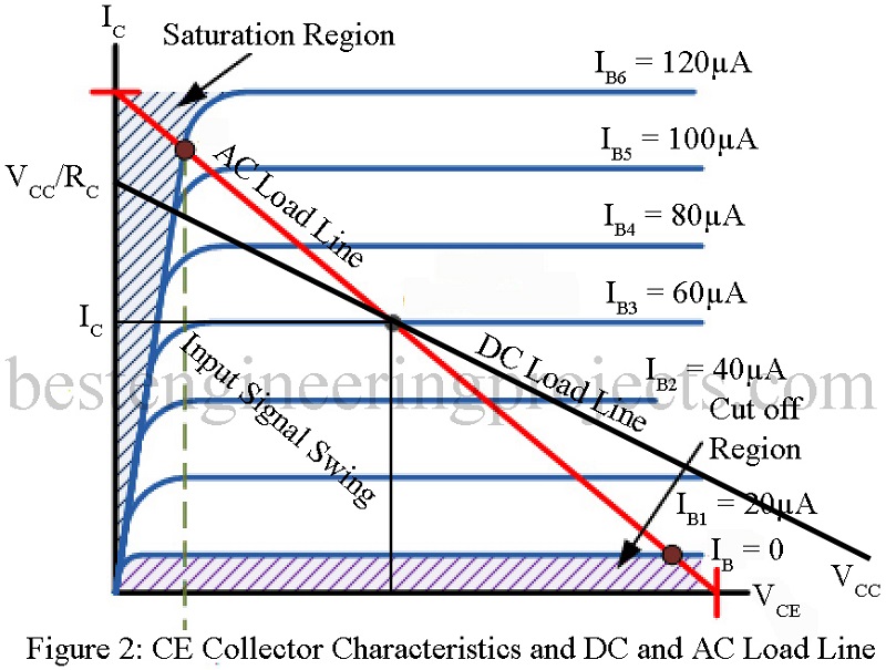
If  , then through the zero-signal operating point P1, we draw an a.c. load line for load resistance RL’ = RL || Rc as shown in figure 3. On application of a time varying input signal (base current), the operating point moves symmetrically about P1 along the a.c. load line. It is evident from Fig. 2 that the maximum swing of the input signal about zero signal point P1 is approximately 40 uA. For larger input signal swing say 60 uA, during negative excursion exceeding 40 uA, the collector current becomes zero.
Thus, this zero-signal operating point P1 serves satisfactorily if the input signal swing does not exceed 40 uA. For larger input signal swing, say 60 uA, a more suitable quiescent operating point has to be selected. In order to avoid cutoff during the low current region of the cycle, the quiescent operating point should be located at a higher current on the dc load line. This selection is by trial and error. Thus, suppose we select P2 as the quiescent operating point as shown in Fig. 2. This permits maximum input signal swing of 60 uA without cutoff in the low current region and without nonlinearity in the high current region.
Fixed Bias Circuit:
Amplifier of Fig. 1 uses fixed bias. In this circuit, the zero-signal operating point P2 may be established by selecting resistance Rb such that the base current IB equals the current IB2 corresponding to the zero-signal operating point P2.
Thus,  …..(3)
But VBE across the forward biased emitter junction JE is very small, being only about 0.2-volt (0.6 volt) in Ge (Si) transistor. Thus VCC >> VBE. Hence neglecting VBE, Equation 3 yields,
 …….(4)
Thus, bias current IB is constant and the circuit constitutes a fixed bias circuit.
Waveforms of output voltage and Current
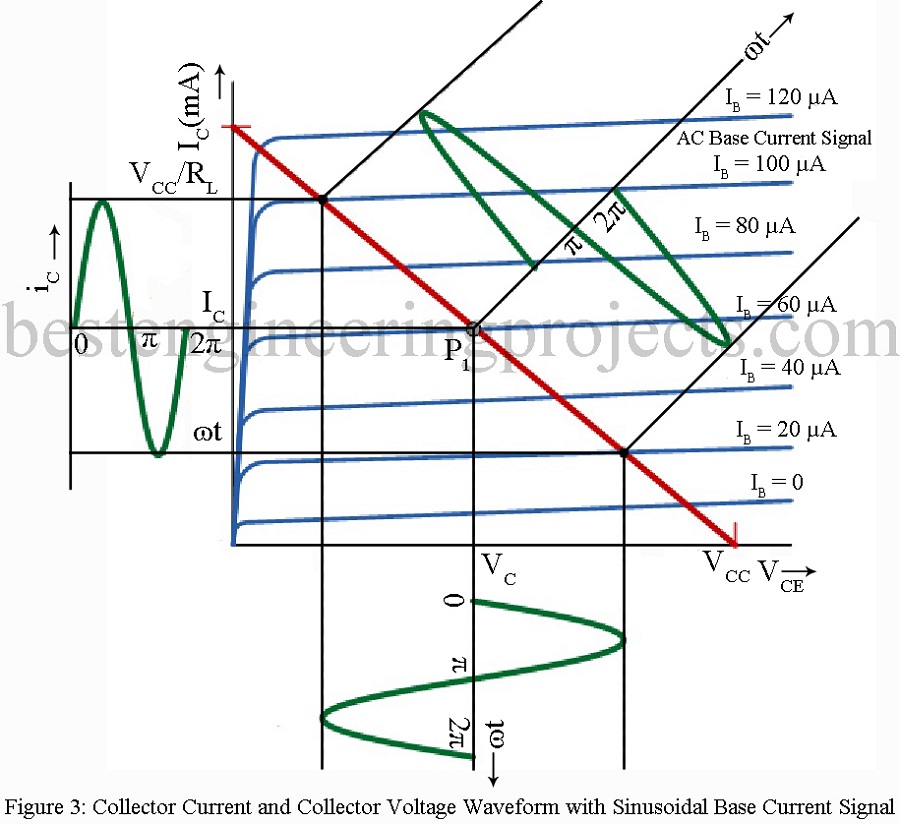
Let  and let P1 be the zero-signal operating point on d.c. load line for base bias current IB = 40 uA as shown in Fig. 3. Let a sinusoidal signal a.c. base current of amplitude 40 uA be applied at the input. This signal gets superimposed on the bias base current IB1 ( = 40 uA). As the base current varies with time, collector current and collector voltage also change with time as shown in Fig. 3. This a.c. collector current forms an amplified version of the input base current.
It is evident that with properly selected zero signal operating point, the output signal is not distorted. In case, the operating point P1 is placed at IB 20 uA, then with input signal current of amplitude 40 uA there results negative peak clipping of collector current iC and similar clipping of collector voltage vC resulting in distortion. similarly, if point P1 is placed at say IB = 80 uA, then again with input signal current of amplitude 40 uA, there results positive peak clipping of collector current and corresponding distortion of collector voltage VC.
ln Fig 3, we have used the d.c. load line. If  , we should use the a.c. load line. In that case, the zero-signal operating point P1 should be selected in the middle of the a.c. load line.
Causes of Shift of Zero Signal (Quiescent) Operating Point
We have seen that proper selection of quiescent operating point in vital for linear amplification. But the quiescent operating point may shift due to the following reasons.
- Change of
 on transistor replacement
 - Thermal variations
Let us consider these aspects.
- Transistor Replacement Discrete transistors of the same nomenclature and manufactured by the same firm have widely different values of device parameters including . Hence when a transistor in a given circuit is replaced by another of the same type, the transistor characteristics change somewhat and the quiescent operating point shifts.
- Thermal Variations. A rise in temperature Causes three effects:
- increase in ICBO (or ICO). Thus, ICBO doubles for every 10°C rise in temperature
- VBE reduces at the rate of 2.5 mV/deg C rise in temperature
- increases with the rise in temperature.
Here apart from ambient temperature variations, internal causes also have to be considered. Thus, any increases in IC causes rise in temperature of collector junction JC which in turn causes rise in ICO. this rise in ICO causes further rise in IC. this in cumulative process and may damage the device unless adequate means are adopted to remove heat from the device. Even when damage of the device does not take place, there results considerable shift of the quiescent operating point i.e. thermal run away is said to take place.
Thus, operating point P may shift from the middle of the active region to saturation. We know that:  . Then even if we assume
  to be temperature invariant, for IB = 0, with increase of temperature, output characteristics of CE transistor move up because of the rise in ICBO. For nonzero value of IB, the IC versus VCE curves also move up by the same amount. Hence the operating point moves up.
Increase of with rise of temperature causes further upward movement of quiescent operating point.
Means of Achieving Operating Point Stability
Operating point stability may be achieved in the following ways:
- By using stabilization methods: use of proper biasing circuit, which permits such a variation of the base biasing current IB as to maintain IC almost constant in spite of variation of ICO, VBE and ..
- By using Compensation methods: use of compensation elements such as diode, transistor, thermistor etc. theses device produce compensating voltage and currents and thus maintain the operating point stable.
Additional means are adopted to maintain the ambient and the junction temperatures constant. Thus, air conditioning or thermostat chamber (wherever possible) may be used to maintain the ambient or case temperature constant. Heat sink and air blast may be used to remove heat from the transistor.
We here take up only a brief study of biasing method for operating point stabilization.
Desired features of Biasing Methods: The biasing circuit used in transistor should be such as:
- To establish conveniently the operating in the middle of the active region of the characteristics.
- To make the operating point independent of transistor parameters.
- To stabilize the collector current against temperature variations.
Different Biasing Methods: Various biasing method possible are:
- Two battery bias
- Fixed bias
- Collector-to-base bias
- Fixed bias with emitter circuit resistor
- Self-bias
Out of theses method, the self-bias is the one most effective and convenient ands is, therefore, almost always used. We, therefore, take up here the study of this biasing method only.
Self-Bias (Emitter Bias)
Figure 4 gives the circuit of CE amplifier using self-bias or emitter bias. This biasing method is most popular used because it produces excellent operating point stability. The d.c. component of current through the resistor Re caused d.c. voltage drop VE in the polarity shown in figure 4. this voltage drop causes a reverse bias at the emitter junction JE. but R1 – R2 combination across the VCC supply produces a positive d.c. voltage Vb at the base relative to the emitter. The net forward bias at the emitter junction JE then equals (Vb – Ve)
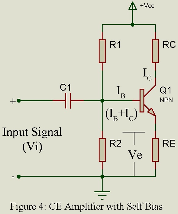
Stabilization Action of Self Bias Circuit Any rise in temperature T causes rise in ICBO and hence rise in IC. This increased current through Re causes increased dc voltage drop across Re and results in reduced net emitter-to-base forward bias, reduced base current Ib and reduced collector current IC. This reduction in IC tends to cancel the rise in IC as caused by temperature rise. Operating point stability is thus improved.