Zener Breakdown and Avalanche Breakdown

volt ampere characteristics of typical Si and Ge zener diode

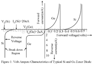
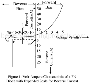
Figure 1 gives the volt-ampere characteristic of a PN diode including the breakdown region. Thus, when a PN diode is highly reverse biased, the junction may breakdown i.e. it presents extremely small resistance with the result that the current increases abruptly at an almost constant voltage. This current may be limited only by placing a suitable resistor in the external circuit. However, the breakdown is not permanent. The diode returns to its normal condition when this large reverse bias is removed. The breakdown of diode may be of two types:…

Read More

Transition Capacitance and Diffusion Capacitance of Diode

Forward biased pn diode

Transition Capacitance CT of Diode (Space Charge Capacitance) With the increase of the magnitude of reverse bias, majority carriers move away from the junction i.e. the width W of the depletion layer increases. This uncovered immobile charge on the two sides of the junction constitute a capacitor of incremental capacitance CT is given by,                ……..(1) Where dQ is the increase in the charge resulting from an increase dV in voltage. Hence, a voltage change dV in the time interval dt will result in a current i was given by,…

Read More

Volt Ampere Characteristic of a PN Diode

volt ampere characteristic of a pn diode with expanded scale for reverse current

What is Volt Ampere Characteristic of PN Diode? Current I in a PN diode in related to the junction voltage VV by the relation given by equation,               ………..(1) Figure 1 gives the typical volt-ampere characteristic for a PN diode plotting above equation. With forward bias, the forward current remains essentially zero until the so called Cutin voltage VV of t diode is reached. This cutin voltage is defined as the voltage below which the forward current is less than 1% of the maximum rated current of the diode. This…

Read More

Forward and Reverse Biased PN Diode

Forward biased pn diode

Here in this article we are going to discuss about forward and reverse biased PN diode. We had also derive the equation and solve a numerical example. At first let’s see the reverse biased pn diode. Reverse Biased PN Diode Figure 1 shows a PN diode with reverse bias i.e. with negative terminal of the battery connected to the P-side of the diode and the positive terminal to the N-side. With the polarity of connection, holes in the P-region and the electrons in the N-region move away from the junction…

Read More

Open Circuit PN Diode

open circuit pn diode

What is Open Circuit PN Diode? Figure 1(a) shows an open circuited pn diode with acceptor impurity density NA in the p-region and donor impurity density ND in the n-region. We assume that each acceptor atom has ionized resulting in one immobile negatively charged acceptor ion and one mobile hole. Similarly, each donor atom has ionized resulting in one immobile positively charged donor ion and one mobile electron. In Figure 1(a) the immobile acceptor ion is indicated by a minus sign enclosed within a circle while immobile donor ion is…

Read More

Types of PN Junction Diode

alloyed junction diode

In this Tutorial we are describing PN diode and types of PN Junction Diode. What is PN Junction Diode? A PN junction or P-N diode consists of a semiconductor having two regions, a p-region and n-region with a junction in between. The junction region or the transition region where the nature of the semiconductor material changes from p-type to n-type is usually very thin, typically 10-6 to 10-4 cm wide depending on the method of concentration. What are the types of PN Junction Diode? Depending on the method of construction,…

Read More