Figure 1 gives the volt-ampere characteristic of a PN diode including the breakdown region. Thus, when a PN diode is highly reverse biased, the junction may breakdown i.e. it presents extremely small resistance with the result that the current increases abruptly at an almost constant voltage. This current may be limited only by placing a suitable resistor in the external circuit. However, the breakdown is not permanent. The diode returns to its normal condition when this large reverse bias is removed. The breakdown of diode may be of two types: (a) zener breakdown and (b) avalanche breakdown.
Zener Breakdown:
In the diode using heavily doped P and N regions, on application of a large reverse bias, zener breakdown may take place due to direct breaking of covalent bonds due to strong electric field at the junction. The new electron-hole pairs so created greatly increase the reverse current at an almost constant value of reverse bias typically below 6 volts for heavily diodes. Due to heavy doping of P and N regions, the width of depletion region becomes extremely small. Then, for an applied reverse bias of voltage as small as 6 volts or less, the field across the depletion region becomes very high, of the order of 106 volt/cm causing zener breakdown.
Avalanche Breakdown:
For moderate doping in a diode, the depletion layer width is quite large so that the reverse bias needed to produce strong field to cause zener breakdown becomes excessively large. In such moderately or lightly doped diodes, the breakdown does not take place through zener breakdown mechanism but uses the mechanism of avalanche multiplication. Then let a thermally generated carrier fall down the junction barrier and acquire kinetic energy from the applied voltage. This carrier on colliding with a crystal ion with high kinetic energy causes rupture of a covalent bond. Such an ionization is called Impact ionization. Now in addition to the original carrier, a new electron-hole pair gets created.
These new carriers, in turn, may also require enough energy from the applied field, collide with crystal ions and generated new electron-hole pairs. Tis process is cumulative and is known as avalanche multiplication. The net result is a large reverse current at an almost constant high voltage drop and avalanche breakdown is said to take place.
Zener Diode (Breakdown Diode)
A zener diode, also called Breakdown diode is an PN diode specially designed for operation in the breakdown region in reverse bias condition. The diode may use either zener breakdown or avalanche breakdown. Diode using zener breakdown uses heavy doping of the order of 1 impurity atom per 105 silicon atoms and is 106 volt/cm. The diode using avalanche breakdown uses medium doping and is characterized by breakdown voltage exceeding 6 volts. However, the word zener is commonly used for all diodes having breakdown characteristics in the reverse direction.

Figure 1 gives the volt-ampere characteristics of typical silicon and germanium zener diodes. Breakdown diode is operated over the breakdown region and the current is limited by an external resistance. The breakdown voltage VZ may be suitably selected by proper choice of doping level.
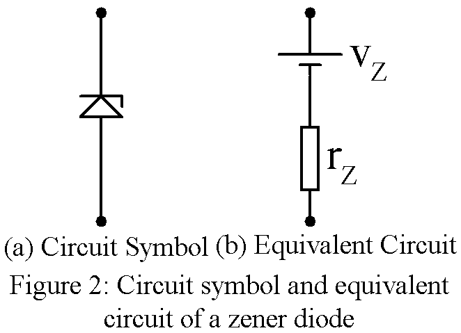
Circuit Symbol and Equivalent Circuit
Figure 2 (a) gives the circuit symbol of zener diode while figure 2(b) gives the equivalent circuit. this equivalent circuit includes a small dynamic resistance and a dc battery of voltage VZ, equal to the zener voltage. The resistor rz represents the resistance corresponding to the slight slope of the nominally vertical region of the characteristic during breakdown. However, in most applications, external resistors are much larger than rz and hence rz may be neglected in the equivalent circuit.
Zener Diode Specifications
Zener Voltage VZ Manufacturers specify the value of breakdown voltage VB, also known as the zener voltage VZ at specific value of test current, Zener diodes are available for value of VZ from 2.5 volts to over 500 volts with accuracies between 5% to 20%.
Power Dissipation It is the product of VZ and IZ. The maximum power rating varies from 150 mW to 250 watts.
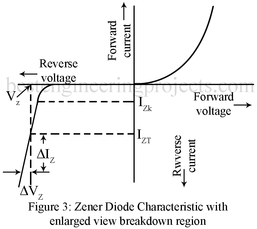
Breakover Current IZK There is some curvature of the reverse breakdown characteristic at low values of IZ. Hence, we specify some value of current near the knee where the voltage across the diode starts to differ appreciably for VZ. Figure 3 shows this current IZK.
Dynamic Impedance This is defined as,
 ………….(1)
Where  and
and  are the increments in VZ and IZ at any pint P on the reverse breakdown characteristic shown in figure 3.
Ideally, the breakdown curve should be a perfect vertical line and rz has a small value ranging from a few ohms to several hundred ohms.
Effect of Temperature on VZ Voltage VZ is influenced by temperature variant. Temperature coefficient of VZ gives the present change in VZ with change in temperature and is defined as,
 ……..(2)
Where  is the change in VZ due to temperature change (T1-T0).
Study of variation of TC with VZ revels that
- TC may be both positive and negative and lies in the range +-0.1 percent per degree C.
- For VZ appreciably exceeding 6 volts characterizing avalanche breaking, TC is positive.
- For VZ below 6 volts characterizing true zener breakdown, TC is negative.
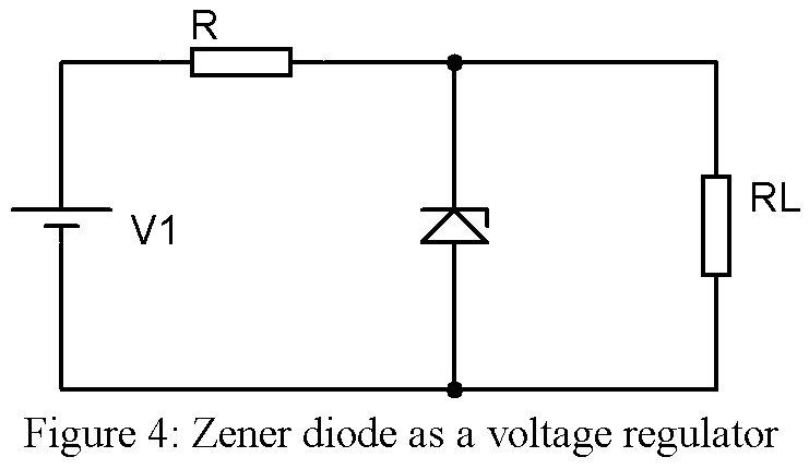
Zener Diode as a Voltage Regulator
Figure 4 gives the circuit using zener diode for providing a constant voltage VZ across load positive RL in-spite of variation in input voltage Vi or load resistance RL. the source voltage Vi and the load resistor RL are so selected that the diode operates in the breakdown region. From figure 4 we find that the voltage VZ across the diode is also the voltage across the load resistor RL and it undergoes very small change in-spite of variation in source voltage Vi or the load current. In fact the zener diode maintains the output voltage VZ constant by adjusting the diode current IZ itself so as to permit a constant load current through RL.