Here in this article we are going to discuss about forward and reverse biased PN diode. We had also derive the equation and solve a numerical example. At first let’s see the reverse biased pn diode.
Reverse Biased PN Diode
Figure 1 shows a PN diode with reverse bias i.e. with negative terminal of the battery connected to the P-side of the diode and the positive terminal to the N-side. With the polarity of connection, holes in the P-region and the electrons in the N-region move away from the junction and the width of the depletion region increases. The height of the potential barrier increases by amount V. This increased barrier height serves to reduce the flow of majority carriers to the other side i.e. holes from P-side to N-side and electrons from N-side to P-side. However, the flow of minority carriers remains uninfluenced by the increased barrier height since these minority carriers fall down the potential energy barrier. As a result, a net small reverse current from a N to P side flows in the diode carried by minority carriers. This small current is the diode reverse saturation current and its magnitude is denoted by I0.

The reverse saturation current I0 is given by,
![I_0 = Aq [\dfrac{D_P}{L_P N_D} + \dfrac{D_n}{L_n N_A}]n_1^2](https://s0.wp.com/latex.php?latex=I_0+%3D+Aq+%5B%5Cdfrac%7BD_P%7D%7BL_P+N_D%7D+%2B+%5Cdfrac%7BD_n%7D%7BL_n+N_A%7D%5Dn_1%5E2&bg=ffffff&fg=000&s=0&c=20201002) ……….(1)
……….(1)
Where A is the cross-section area of the device
DP(Dn) is the diffusion constant for holes (electrons),
LP(Ln) is the diffusion length of holes (electrons)
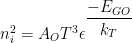
ND(NA) is the donor (acceptor) impurity density and ni is the intrinsic concentration of holes and electrons.
Intrinsic Concentration ni is given by below equation
 ………(2)
Equation (2) may also be put as,
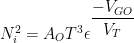 ………..(3)
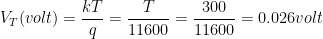
Where VGO is the voltage (in volts) numerically equal to the forbidden gap energy EGO in eV, and VT is the volt equivalent of temperature.
Value of I0 depends on the property of P and N regions and on the operating temperature. At room temperature (300 K), I0 is typically about  for Ge diode and about 1 nA for Si diode. This reverse saturation current I0 is independent of the magnitude of the reverse bias but increase with the increase of temperature T.
Forward Biased PN Diode
Figure 2 shows a PN diode with forward bias V i.e. with positive terminal of voltage source V connected to the P-side and the negative terminal to the N-side. With this forward bias, the holes in the P-region and the electrons in the N-region move closer to the junction. The width of the depletion region reduces and the barrier potential reduces to (V0-V). This reduced barrier potential results in increased flow of majority carrier holes across the junction from P-side to N-side and majority carrier electrons from N-side to P-side. These two current components crossing the junction add up to form conventional electric current across the junction from P-side to N-side i.e. the forward direction and is given by,
 ………(4)

However, the flow of minority carriers remains unaltered by the reduction in barrier potential since the minority carriers fall down the barrier. Thus, the reverse current remains unaffected and equals the reverse saturation current I0 given by equation (1). Hence the net forward current is given by,
![I = I_F-I_0 = I_0[\epsilon^{\dfrac{V}{V_T}}-1]](https://s0.wp.com/latex.php?latex=I+%3D+I_F-I_0+%3D+I_0%5B%5Cepsilon%5E%7B%5Cdfrac%7BV%7D%7BV_T%7D%7D-1%5D&bg=ffffff&fg=000&s=0&c=20201002) ……….(5)
……….(5)
Equation (5) is the semiconductor diode equation and applies for both positive and negative values of the applied voltage V i.e. for both forward bias and reverse bias. For reverse bias, V is negative and is much larger than VT ( 0.026 volt) and hence I equals I0.
Equation (5) ignores the effect of carrier generation and recombination. Such an omission is valid for Ge device but not for Si device. Hence, a more general expression for current I in a PN diode is,
![I = I_0 [\epsilon^{\dfrac{V}{\eta V_T}}-1]](https://s0.wp.com/latex.php?latex=I+%3D+I_0+%5B%5Cepsilon%5E%7B%5Cdfrac%7BV%7D%7B%5Ceta+V_T%7D%7D-1%5D&bg=ffffff&fg=000&s=0&c=20201002) ………..(6)
………..(6)
Where  for Ge and 2 for Si diode at the rated currents.
Equation (5) shows that the forward current increases exponentially with forward voltage V available across the junction.
Large Forward Bias | Forward and Reverse Biased PN Diode
With a large forward bias V say equal to V0, the potential barrier becomes zero and very large current in excess of diode current rating tends to flow. In actual practice, however, current gets limited by the bulk resistance of the diode and the resistance of the ohmic contacts. Hence, only a small part of the applied forward bias V appears across the PN junction and the current is mostly governed by this total device resistance. Since this total device resistance is constant, the volt-ampere characteristic is almost a straight line.
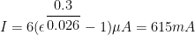
Example 1: in a Ge diode, reverse saturation current I0 is  . Calculate the forward current for forward voltage of 0.2, 0.3 and 0.4 volt at room temperature of 300 K.
Solution:


At V = 0.2 volts,

At V = 0.3 volts,
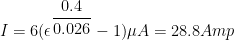
At V = 0.4 volts,
Tutorial Problem
In a Ge diode, reverse saturation current is  . Calculated the forward current for forward voltage of 0.05-volt, 0.1 volt and 0.2 volt at room temperature of 300 K.
[Ans:  ,
, 
 ]
]