Transistor static characteristics curves are nonlinear. But for small signal operation, the point of operation moves about the quiescent operating point over a small range. Then the transistor parameters may be considered to be constant over this small range of operation.
Derivation of h-Parameter model for transistor
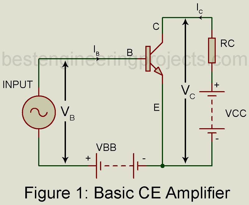
To drive the h-parameter model for a transistor, we consider the basic CE amplifier circuit of figure 1. The variable iB, iC, vB (=vBE) and vC(vCE) represent the instantaneous total values of currents and voltages. The input current iB and output voltage vC are chosen as the independent variables. Then varibles vB and iC are functions of iB and vC. we may write
 …..(1)
 …..(2)
Making Taylor series expansion of equation (1) and (2) about the zero signal operating point (IB, Vc) and neglecting the higher order terms we get,
 …..(3)
 ……(4)
……(4)
When partial derivatives  and
and  are taken keeping the collector voltage constant while partial derivatives
  and
and  are taken keeping the base current constant.
Quantities  ,
,  ,
,  and
and  represent small increments in base and collector voltages and currents and may be represented by the symbols vb, ic, ib and vc respectively. Then we may rewrite Equations (3) and (4) as below:
 ……(5)
……(5)
 ……(6)
……(6)
Where  …..(7a)
 ……(7b)
 ……(7c)
 …..(7d)
The partial derivatives in Equations (7) define the h-parameters of the transistors in the CE configuration.
Parameters hfe is the most important small signal parameters of a transistor and is called small signal  , indicated by ‘ (as already defined earlier).
In case of sinusoidal voltage are currents, Equation (7a) becomes,
 …..{8}
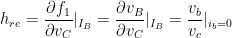
Figure 2 gives the h-parameter model for a transistor in CE configuration. Assuming sinusoidal voltages and currents, rms value Ib, Ic, Vb and Vc have been used. Exactly similar models may be drawn for CB and CE configurations using h-parameters relevant for the configurations.
The model of Equation (3) and the corresponding equations are valid for both PNP and NPN transistors and are independent of the load impedance of the method of biasing.
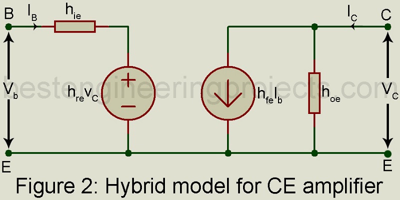
Figure 3 gives the h-parameter models for the transistor in CB and CC configurations. It may be noted that in CC configuration of figure 3(b), B and C are the input terminals while E and C are the output terminals.
Equations (5) and (6) are valid for CE model of figure 2. Similar equations using CB and CC h-parameters may be written respectively for CB and CC models.
For each of the three configurations, application of Kirchhoff’s current law (KCL) gives that the sum of current Ib + Ic + Ie = 0.
The models of Figures 2 and 3 are corresponding equations are valid for both NPN and PNP transistors and are independent of the nature of load impedance or the method of biasing.
Graphical Determination of h-parameters
Static input characteristic curves may be used to determine graphically the parameters hie and hre using equations 7(a) and 7(b) respectively. Similarly, static output characteristic curves may be used to determine hfe and hoe using Equations 7(c) and 7(d) respectively.
Variation of transistor h-parameters
All the four h-parameters for any transistor configuration, namely CE, CB and CC, vary with variation of collecto0r current IC and collector junction temperature. Usually IC = 1mA is taken as the refence collector current. Similarly, collector junction temperature Tj = 250 is taken as the reference temperature.
Value of h-parameters of a Typical Transistor
Table 1 gives the value of h-parameters of a typical transistor for CE, CB and CC configurations.
Table 1 Values of h-parameters of a Typical Transistor |
||||
| S.N. | Parameter | CE | CB | CC |
| 1. | hi | 1100Ω | 22Ω | 1100Ω |
| 2. | hr | 2.5×10⁻⁴ | 3×10⁻⁴ | 1 |
| 3. | hf | 50 | -0.98 | -51 |
| 4. | h0 |  |
 |
|
| 5. | 1/h0 | 40 kΩ | 2 MΩ | 40 kΩ |
Conversion Formulas for h-parameters in the three Configurations
Some manufacturers provide only the four CE h-parameters while other provide hfe, hib, hob and hrb. It is, therefore, often necessary to convert from one set of h-parameters in one configuration to another set in another configuration. Table 2 gives the approximate conversion formulas for h-parameters. These formulas give reasonably accurate results and may be used in almost all cases.
Table 2 Approximate Conversion Formulas for h-parameter |
|
 |
 |
 |
 |
 |
 |
 |
 |
Table 2 enables us to compute CC and CB h-parameters if CE h-parameters are known. The expression for CE h-parameters in terms of CB h-parameters may be obtained from Table 2 on interchanging the subscripts b and e.