Today, many gadgets use touch control – a simple touch makes things happen and adds a modern touch. People who enjoy electronics are creating their power supplies with LM317 variable IC regulators and special switches for power adjustments.
There’s a cool project here called the “Programmable Touch Power Supply Circuit” It’s not just a regular power supply – it has touch magic. You can change settings by touching it, mixing tech with simplicity.
Imagine devices without buttons – this project uses touch sensors. No searching for buttons – just touch and things work. Your gadgets become friends.
For description, we had to divide the entire circuit into various subtopics
Building Blocks of Programmable Touch Power Supply Circuit
AC-DC Converter
The initial step involves transforming high-voltage AC mains input into a lower-voltage format using a step-down transformer. We employ a 230V AC primary to 0-15V AC, 2amp secondary transformer for a 50Hz power supply, or a 110V AC primary to 0-15V AC, 2amp secondary transformer for 60Hz according to your mains voltage. To manage power flow and safeguard against overcurrent conditions, an ON/OFF switch along with a 500mA series fuse is connected to the primary side of the transformer.
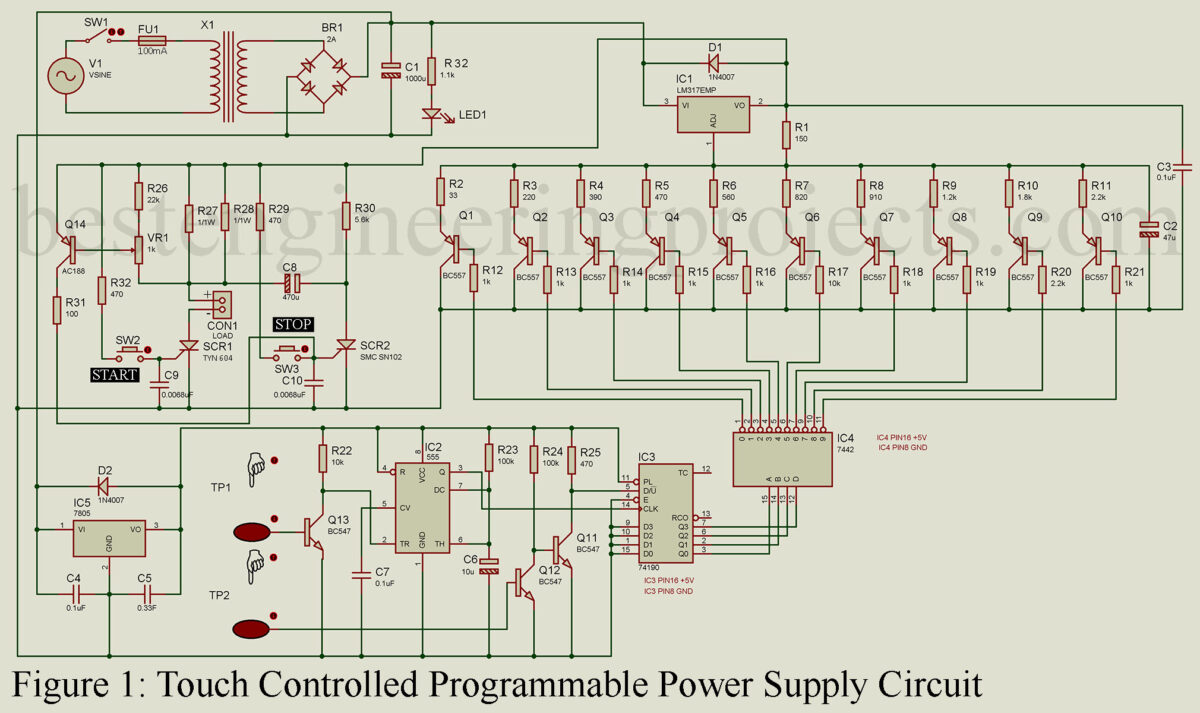
The reduced voltage AC input is then directed to the AC input of a bridge rectifier, resulting in the generation of pulsating DC at the output. A 2A-rated bridge rectifier is employed for this purpose. Despite this conversion, the output DC exhibits ripples and is not entirely smooth. To address this, an electrolytic capacitor with a capacitance of 1000uF is introduced for filtering purposes.
Incorporated within the circuit is an LED indicator that serves to signify the presence of a mains supply, providing a visual cue regarding the availability of power.
Variable Regulated Power Supply Circuit
The positive DC voltage is given to the input pin i.e. 3 of variable voltage regulator LM317 as shown in the circuit diagram. The output voltage from the output of the LM317 is selected by transistor T1 to T10 with the help of resistor R2 through R11. These transistors are made to switch on and off turn by turn instead of a single pole 10-way rotary switch. The transient response of the power supply is improved by capacitor C2 and 50/60 Hz hum is filtered by capacitor C3.
The output positive DC voltage is connected to the input pin, designated as pin 3, of the LM317 variable voltage regulator. This arrangement can be visually understood through the provided circuit diagram.
Subsequent to this, the output voltage coming from the LM317 unit is selected through an arranged series of transistors ranging from T1 to T10 with the help of resistors ranging from R2 to R11. Instead of the conventional methodology employing a single-pole 10-way rotary switch, this arrangement introduces a systematic, sequential switching mechanism wherein the transistors are cyclically involved and free to achieve the desired voltage output.
To extend the transient response of the power supply and better the impact of unexpected voltage transitions, the inclusion of capacitor C2 serves as a vital component. This capacitor effectively moderates the adverse effects of rapid voltage fluctuations, thereby enhancing the overall stability of the power supply system.
Additionally, the predominant phenomenon of 50/60 Hz hum, stemming from the AC power source, is effectively moderated through the integration of capacitor C3. As a proficient filtering agent, C3 adeptly attenuates the undesirable harmonic artifacts linked to the hum, resulting in a refined and harmonious output profile.
Touch control circuit
The touch sensor circuit is built around a touch plate and the NE555 integrated circuit (IC). The NE555 timer IC operates as a monostable multivibrator in this configuration, producing an output pulse with a duration slightly exceeding one second. Two transistors, Q13 and Q12, have their bases linked to distinct touch plates, TP1 and TP2, correspondingly, as depicted in the circuit diagram.
Upon interacting with touch plate TP1, the inherent 50Hz body hum starts conduction in transistor Q13. Consequently, the NE555 timer IC is triggered. The output (from pin 3) of the NE555 is supplied to the Clock (CLK) input (Pin 14) of the UP/DOWN decade counter IC 74190 (IC3). Another touch plate, TP2, is associated with the UP/DOWN input (Pin 5) of IC3 through a pair of transistors, Q12 and Q11.
The functionality of counting in the upward or downward direction is reliant on three pins of IC3: Load (Pin 11), U/D (Pin 5), and CLK (Pin 14). The essential operational characteristics are clarified through the utilization of a truth table.
Truth Table
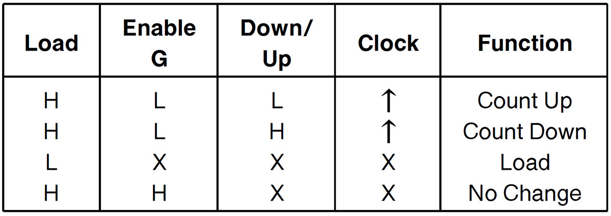
For the purpose of executing either upward (UP) or downward (DOWN) counting, it is imperative that the Load pin (Pin 11) be maintained in a High state, thereby connected to a 5V power supply. The 74190 IC, characterized by its low-enable feature, necessitates grounding the Enable pin (Pin 4). The UP/DOWN pin (Pin 5) governs the counting direction: a low state triggers UP counting, while a high state initiates DOWN counting, dependent upon the application of clock pulses.
In accordance with the established circuit configuration, the initial state of Pin 5 is low. In this particular scenario, every touch interaction with TP1 produces a voltage output modification in an ascending manner. Conversely, appealing TP2 transitions Pin 5 of IC3 to a high state or logic 1. Consequently, utilizing TP1 causes the output voltage to undergo successive decrements.
The outputs emanating from Q0, Q1, Q2, and Q3 of IC3 (74190) are inserted with the four inputs, A, B, C, and D, of IC4 (7442). The IC 7442 functions as a 4-line to 10-line BCD to Decimal Decoder, a module that translates its four-line input into a singular, sequential output based on the input configuration. Each of the outputs from IC4 is related to the base of ten distinct transistors via individual resistors, as described in the circuit diagram. Thus, these transistors are effectively governed through touch-based switches, writing their operational behavior.
Short Circuit Protection Circuit:
The implementation of the short circuit protection circuit involves the incorporation of two Silicon Controlled Rectifiers (SCRs), as visually depicted in the circuit diagram. The circuit is enhanced with the inclusion of two push-to-on switches, serving the dual purpose of initiating and halting the connected loads.
Parts List of Programmable Touch Power Supply Circuit
Resistors (all ¼-watt, ± 5% Carbon unless stated)
R1 = 150 Ω
R2 = 33 Ω
R3 = 220 Ω
R4 = 390 Ω
R5, R25, R29, R32 = 470 Ω
R6 = 560 Ω
R7 = 820 Ω
R8 = 910 Ω
R9 = 1.2 KΩ
R10 = 1.8 KΩ
R11 = 2.2 KΩ
R12 – R21 = 1 KΩ
R22 = 10 KΩ
R23, R24 = 100 KΩ
R26 = 22 KΩ
R27, R28 = 1 Ω, 1W
R30 = 5.6 KΩ
R31 = 100 Ω
R32 = 1.1 KΩ
VR1 = 1 KΩ (potentiometer)
Capacitors
C1 = 1000µF/50V electrolytic
C2 = 47µF/50V electrolytic
C3, C4, C7 = 0.1µF ceramic
C5 = 0.33µF ceramic
C6 = 10µF/25V electrolytic
C8 = 470µF/25V electrolytic
C9, C10 = 0.0068µF ceramic
Semiconductors
IC1 = LM317T voltage regulator
IC2 = NE555 timer
IC3 = 74190 up/down decade counter
IC4 = 7442 BCD-to-decimal decoder
IC5 = LM7805, +5V regulator
BR1 = 2A Bridge rectifier
D1, D2 = 1N4007 silicon diode
T1 – T10 = BC557 pnp transistor
T11 – T13 = BC547 npn transistor
T14 = AC188 pnp transistor
SCR1 = TYN 604
SCR2 = SMC SN102
Miscellaneous
X1 = 230V AC primary to 0-15V AC, 2amp secondary transformer
SW1 = On/off switch
SW2, SW3 = push-to-on switch
TP1, TP2 = Touch Plate
100mA fuse
LEDs
It looks to be very important program that is useful for our daily needs for the purpose of going through the current nerds