Resistance Capacitance Coupled or R.C. Coupled Amplifier
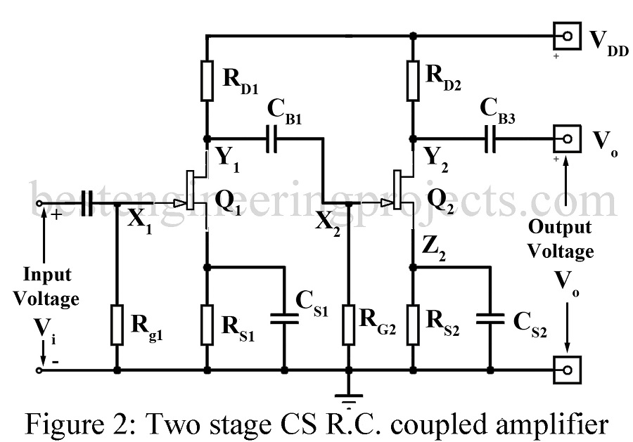
Figure 1 gives the circuit of a two-stage common emitter R.C. coupled amplifier while figure 2 gives the circuit of a two-stage common source (CS) FET R.C. coupled amplifier. Typical component values are also indicated.
In both amplifier circuits of Figure 1 and 2, X1 and Y1 are the input and output terminals of the first stage. The output at Y1 is coupled to the input X2 of the second stage through a coupling capacitor Cb2. This capacitor serves another function of blocking the dc component at Y1 from reaching X2. Resistor Rc (Rd) forms the load resistor in the collector (drain) circuit. In the figure 2, Rg1 extends from gate to the ground. This resistor together with Rs1-Cs1 provides the desired bias. In figure 3, emitter circuit resistor Re1 along with potential divided resistor R11 and R12 provides the desired emitter bias.
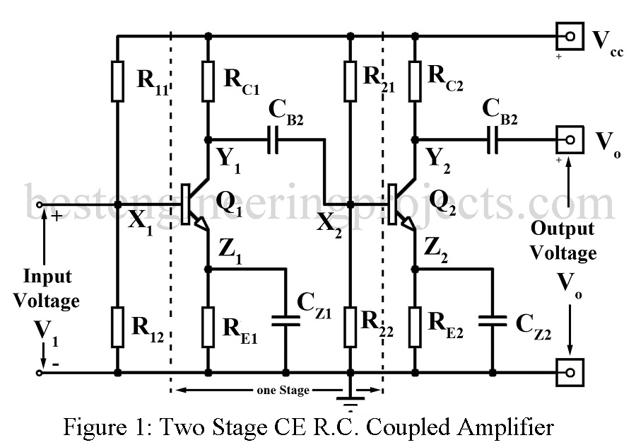
In figure 1 and 2, high value bypass capacitor CZ1 (CS1) offers an almost short circuit even to the lowest frequency component and thus prevent loss of amplification due to negative feedback. The high frequency response of the amplifier depends on (i) junction capacitance (ii) capacitances associated with the device sockets and proximity of the components to the chassis and (iii) signal leads. For the purpose of analysis, we assume that the active device (BJT or FET) functions linearly permitting use of small signal models.
Frequency Response | Resistance Capacitance Coupled or R.C. Coupled Amplifier
For the purpose of analysis, we may replace the amplifying device (BJT or FET) by its small signal equivalent circuit and then resort to the technique of network analysis.
The entire frequency range may be divided into following three categories:
(a) low frequency range (b) Middle frequency range or midband (c) High frequency range
In the midband, the voltage gain AVm, current gain AIm and phase delay remain almost constant. The low frequency range lies below the midpoint and, in this range, analysis may be done on replacing the transistor (or FET) by its small signal low frequency model. Shunt capacitance may be neglected in the low frequency range.
The high frequency range lies above the midband and in the frequency, the analysis may be done on replacing the transistor (or FET) by its small signal high frequency model. The junction capacitances of the device and so also the stray shunt capacitance have to be considered in the analysis. However, the coupling capacitor Cb may be neglected.
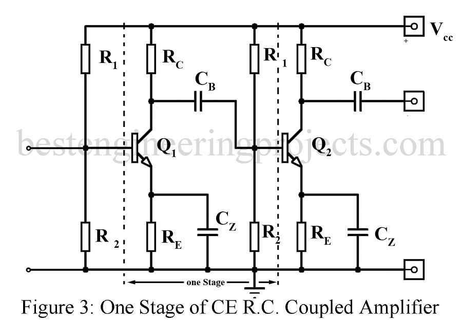
One stage of a multistage BJT amplifier is generally taken from the input i.e. base of one BJT to the base of the BJT in the next stage as shown in figure 1 reproduced in figure 3.
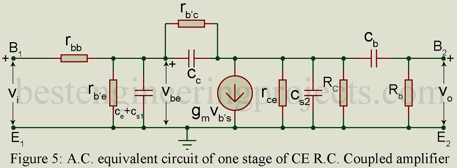
Analysis may be done using an a.c. equivalent circuit for BJT. The circuit most popularly used today is the high frequency hybrid- model for the BJT shown in figure. here rbb’ is the base spreading resistance and B’ is the internal base.
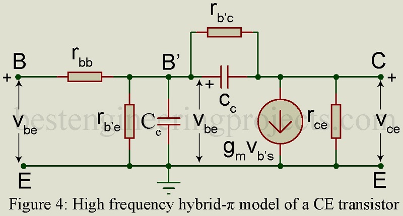
On replacing BJT in figure 3 by the high frequency hybrid- model of figure 4, the high frequency equivalent circuit for one stage of RC coupled amplifier may be drawn as in figure 5 CS1 and CS2 represent the stray capacitances as may be caused by wiring, proximity (closeness) of components to chassis etc.
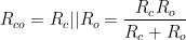
Equivalent circuit of figure 5 is modified using simplifying assumptions and ultimately, we arrive at the amplified a.c. equivalent circuit shown in figure 6.
In figure 7, C represents the total effective shunt capacitance on the input side and is given by,
 …..(1)
 ……(2)
……(2)
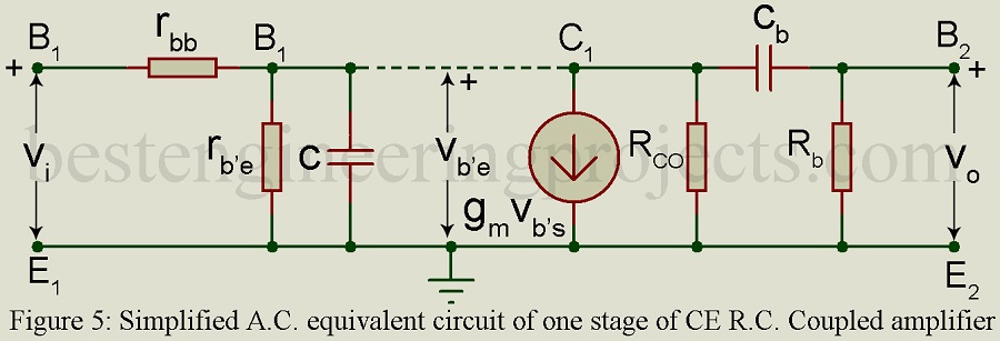
Where Ro represent rce and approximately equals 
 …..(3)
Analysis (not taken up here) of this one stage of RC coupled amplifier using equivalent circuit of Figure 6 gives the following results:
(A) Middle Frequency Range (Mid-band)
Current gain 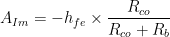 …..(4)
Voltage gain  …..(5)
Where Rcob is parallel combination of Rco and Rb and equals 
From equation (4) and (5) we find that the current gain AIm and the voltage AVm are constant in the middle frequency range.
(B) Low Frequency Range:
In the low frequency range, frequency begin small, reactance of shunt capacitor C is extremely large. Hence C may be omitted from the equivalent circuit of Figure 7. But the reactance of coupling capacitor Cb is quite large. Hence Cb cannot be omitted. In fact, it is the presence of Cb which cause reduction of gain in the low frequency range.
Current gain  …..(6)
Where 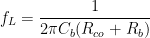 …..(7)
Magnitude 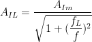 …..(8)
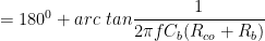
Phase angle of current gain at any frequency f is,
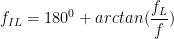 …..(9)
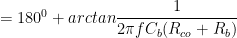 …..(10)
At 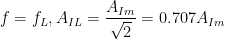 . Thus at fL AIL is 3 dB below AIm.
Hence fL forms the lower 3-dB or lower half power frequency for current gain.
Voltage gain 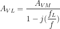 …..(11)
Where  …..(12)
Magnitude 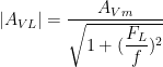 …..(13)
Phase angle 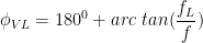 …..(14)
 ……(15)
Thus lower 3-dB frequency for current is the same as the lower 3-dB frequency for voltage gain.
(c) High frequency range:
In the high frequency range, frequency being large, reactance of the coupling capacitance Cb is extremely small. Hence Cb may be omitted. However, reactance of shunt capacitance C is quite small. But C cannot be neglected. In fact, C, being in the shunt path, causes drop in current gain and voltage gain in high frequency range.
Current Gain 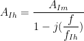 ……(16)
Where, 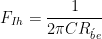 (17)
(17)
Magnitude 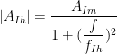 …..(18)
Phase angle of current gain at any frequency f is,
 …..(19)
 ……(20)
At f = fIh =  = 0.707 A_{Im}[/latex].
Thus, fIh forms the higher 3-dB frequency for current gain.
Voltage Gain  …..(21)
Where  ……..(22)
Where  …..(23)
Magnitude 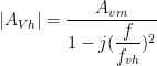 …..(24)
Phase angle of voltage gain Avh at any frequency f is,
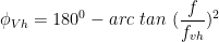 …..(25)
 ……..(26)
At 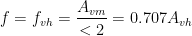 .
.
Thus, Avh forms the higher 3-dB frequency for voltage gain.
Frequency Response Curve
Figure 7 gives the voltage gain versus frequency curve for one stage of CE RC coupled amplifier in the low, middle and high frequency ranges. This forms the frequency response curve. Actually the gin  or
or  expressed in decibels i.e.
  and
and  are plotted along the y-axis on linear scale against frequency f on log scale. Thus, effectively the gain versus frequency is plotted on log-log scale. Thus, curve is called the Bode magnitude plot.
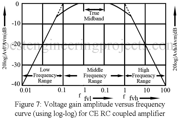
Bandwidth 3-dB bandwidth: or simply the bandwidth B of an amplifier is the frequency range extended from lower 3-dB frequency fVL to higher 3-dB frequency fvh. In this frequency range, the magnitude of the gain remains almost constant ignoring the 3-dB variation. In most cases fvh >> fvL. Hence, Bandwidth B = fvh – fvL = fvh
True Mid-band true midband extends for 10 fvL to 0.1 fvh in which frequency range, gain Av remains truly constant.
If we plot | | or |
 | in dB against frequency f on log scale, again we arrive at the curve in Figure 10.11. Corresponding 3-dB bandwidth is then,
 ……(27)