A signal which contains almost all frequencies is called white noise. In an audio system white noise contains only audible frequency. The white noise of the electrical system is analogous to white light from optics, where white light contains all frequencies or colors. White noise is mostly used in the testing audio equipment like pre-amplifier, power amplifiers, filters, etc. Check out the article on Electrical noise | Types of Electrical Noise. So, today in this article we are going to describe a simple white noise generator circuit. This circuit can use up to 100kHz frequency.
Simple White Noise Generator Circuit Description
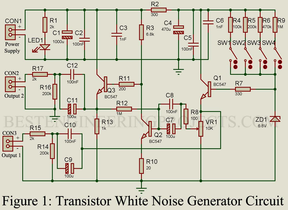
The Simple White Noise Generator Circuit is designed around general-purpose Bi-polar NPN transistor BC547. BC547 is available in the TO-92 package and its three-pin are arranged as collector, base, and emitter.
The main purpose of selecting BC547 are:
- High DC gain (800 max).
- Cheap and easily available
- Low base current (5mA max).
- The base-emitter is about 6V where the collector-emitter voltage is about 65V.
A Zener diode is used here in order to generate noise. While selecting the Zener diode few considerations should be kept in mind.
- The breakdown voltage of the Zener diode must be less than the power supply voltage.
- If the power supply voltage is between 12V to 15 the breakdown voltage of the Zener diode will be 6.8V.
- If the power supply voltage is between 9V and 12V then the breakdown voltage of the Zener diode will be less than 6V.
The current through the Zener diode is responsible for generating noise. Here, to control the current through the Zener diode, four switches are used to select the desired current and get desired noise power.
Simple white noise generation technique
The noise output from Zener is given to the base of transistor Q1, Transistor T1 is configured as a common collector amplifier or we can also say, emitter follower. As the input of the common collector must have high input resistance and output must have low resistance. At very low current Zener diode offers very high resistance at the input side of transistor Q1. At the output, there is no external resistance connected, thus having very low resistance. The gain of the common-collector amplifier is unity i.e. one. Therefore, the output of transistor Q1 is the same as the input noise amplifier. Thus you can also say the output of transistor Q1 is a buffer of input noise.
In case we need to amplify white noise we have to add a further amplifying stage.
White Noise Generator Circuit with an amplifier
In the second circuit, we further add an amplifier built around transistors Q2 and Q3 as shown in the figure below. Variable resistor VR1 is used here to adjust the amplitude of amplified noise.
Transistor Q2 is configured as a voltage amplifier or we can say common emitter amplifier. The voltage gain of the common emitter amplifier
Check out the article Common Emitter Amplifier for other different parameters. From the above expression, we can say that resistor connected at the collector and the resistor connected at the emitter is responsible for voltage gain. With the above configuration, the output voltage i.e. voltage at the collector is about half of the supply voltage. The output of transistor Q2 is connected to the base of transistor Q3 through a resistor R11. Transistor Q3 is also configured as a common collector amplifier.
Output at connector CON3 is buffered white noise where output at CON2 is amplified version of white noise. If you need high white noise power, you have to change the transistor with a power transistor and the Zener diode with a high power Zener diode.
The supply voltage will be 15V but this circuit will work fine with 12V also. In case if the supply voltage is changed to 9V then the breakdown voltage of the Zener diode will be less than 6V (say 5.8V).
PCB Diagram
PCB Diagram is designed using Altium Design software. The solder side PCB diagram and the component side PCB diagram is shown in figure 2 and 3 respectively, where 3D design is shown in figure 4.
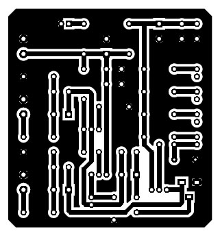
Figure 2: Solder Side PCB Diagram
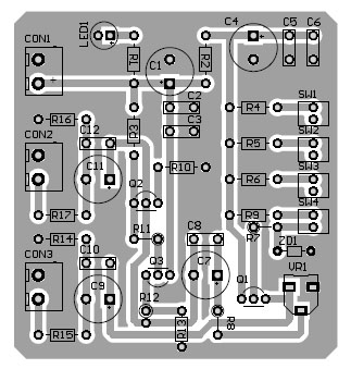
Figure 3: Component Side PCB
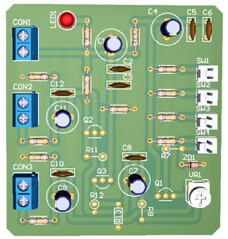
Figure 4: 3D view of White noise generator circuit
Components Required for Simple White Noise Generator Circuit
| Resistor (all ¼-watt, ± 5% Carbon) |
| R1, R15, R17 = 2kΩ
R2 = 330Ω R3 = 6.8kΩ R4 = 100kΩ R5, R14, R16 = 200kΩ R6 = 470kΩ R7 = 330Ω R8 = 100Ω R9, R12 = 1MΩ R10 = 20Ω R11 = 200Ω R13 = 1kΩ VR1 = 10K Potentiometer |
| Capacitors |
| C1 = 1000µF, 25V
C2, C5, C8, C10, C12 = 100nF C3 = 1nF C4, C6 = 470µF, 25V C7, C9, C11 = 100µF, 25V |
| Semiconductors |
| Q1 – Q3 = BC547
ZD1 = 6.8V Zener diode LED1 = 5mm ant color LED |
| Miscellaneous |
| SW1 – SW4 = ON/OFF Switch or 4 channel DIP switch
Connector for input and output |