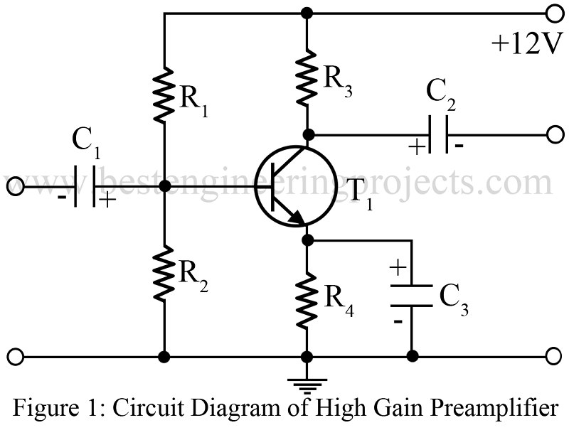
The project posted here is of a high gain preamplifier circuit with a low input impedance of about 4 KΩ. It is capable of very high gain in the order of a few hundred if Rc is very greater than RL.
Circuit Description of High Gain Preamplifier Circuit
The circuit of the high gain preamplifier is built around a low-power NPN transistor T1 which is here configured in common emitter mode using self-bias or emitter bias. This biasing method is used because it produces excellent operating point stability.

Resistor R1 and R2 combination cross the Vcc supply and produce a positive dc voltage at the bias relative to the emitter. As in a simple preamplifier circuit, the input signal is given to the base of transistor T1 through coupling capacitor C1. The dc component of current through the resistor R4 causes a dc voltage drop, which causes reverse bias at the emitter junction. In the circuit high gain preamplifier, high-value bypass capacitor C2 offers an almost short-circuit even to the lower frequency component and thus prevents loss of amplification due to negative feedback.
Check out other preamplifier circuits posted in bestengineeringprojects.com
- Dynamic Microphone Preamplifier Circuit
- JFET Op-Amp Based Stereo Control Preamp
- Electric guitar preamp circuit
- Preamplifier for ceramic-pickup
- Simple Preamplifier Circuit using Single Transistor
PARTS LIST OF HIGH GAIN PREAMPLIFIER CIRCUIT
| Resistor (all ¼-watt, ± 5% Carbon) |
| R1 = 180 KΩ
R2 = 33 KΩ R3 = 3.9 KΩ R4 = 1 KΩ |
| Capacitors |
| C1, C3 = 10 µF, 25V (Electrolytic Capacitor)
C2 = 100 µF, 6V (Electrolytic Capacitor) |
| Semiconductor |
| T1 = BC148B (low power silicon NPN amplifier transistor) |