In the article “PWM DC Motor Speed Controller Circuit” article, we will learn, how to control motor speed using a comparator IC. This circuit has an advantage over a normal motor speed controller using 555 timer IC i.e. it protects MOSFETs from short-circuits. This speed control is accomplished in three phases using two methods: variable switching frequency and variable pulse width modulation. The phases are explained as follows:
- We will first produce square wave pulses of the necessary frequency i.e. switching frequency.
- We will create PWM pulses of the required width in the second stage. The pulse width will be modified to regulate the length of time for which the motor will be ON, resulting in variable speed control.
- Finally, we initiate motor actuation in the third step.
Circuit Description of PWM DC Motor Speed Controller Circuit
Comparator IC :
The introduction to Comparator IC, its key parameters, and its application is explained in: Comparator IC | Parameters and Applications. In this DC motor speed controller project the LM339 comparator IC will be used, which contains four independent voltage comparators, out of this we are using two comparators in this project.
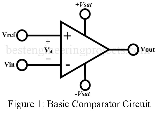
If you need to generate multiple oscillating signals or execute many simultaneous comparator operations with a short response time, the LM339 is a good choice. A voltage comparator, as shown in Figure 1, determines the difference between two input voltages and simply outputs a positive or negative saturation limit. Because the comparator’s output is tuned for saturation, it is truly similar to a 1-bit ADC. The output logic level (i.e. +Vcc/-Vcc or +Vsat/-Vsat) is determined by the voltages applied in the comparator’s power rails.
Comparator as Square wave oscillator
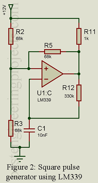
With the help of LM339, we can build an oscillator for a frequency of a few megahertz. A symmetrical square wave generator using minimum components is shown in figure 1. The frequency of the oscillator is determined by the RC time constant of resistor R14 and capacitor C1, where the total hysteresis of the loop is set by voltage divider resistors R2, R3, and positive feedback resistor R5. Initially, the output of the oscillator is high then the capacitor starts to charge through the negative feedback resistor R12. Resistor R11 is a pull-up resistor and is used to ensure the output voltage will go all the way up to +Vcc in the high state. This resistor also avoids crossover distortion in the output waveform. While choosing this resistor, keep in mind that its value must be very low.
The mathematical calculation involves the frequency calculation
The voltage at the positive input pin
From above figure we can see that
R2 = R3 = R5
Thus,
When the voltage of capacitor C1 reached V+, the output of the comparator switched to ground i.e. 0V. After that, the capacitor starts to discharge till the voltage of the capacitor reached half of V+ i.e. () through the same resistor i.e. R12. After that output of the comparator switch to +Vcc and as a result capacitor start to charge. This process is continuous.
The expression of V+ can be expressed as
Rearranging the equation
Taking natural logarithm in both side
This is the expression of the charging time period of capacitor C1. The charging time and discharging time of capacitor C1 are the same.
The total time period is the sum of the charging time and discharging time of capacitor C1. Thus,
Total time period = t1 + t2 = 2t1
Therefore .
Frequency .
From figure , the value of resistor R = 330K and capacitor C = 10nF. By putting the value of RC in equation 1, we can calculate the value of frequency
Variable Pulse Generator
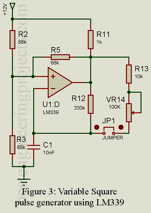
The circuit of the variable pulse generator is shown in the figure. A variable resistor of 100K is connected in series with a 10K resistor. These two series resistor network is connected in parallel to negative feedback resistor R12 as shown in the figure. For a variable pulse, the jumper should be shorted and for a fixed pulse, the jumper should be open.
Condition 1: When wiper of variable resistor at minimum side
Total series resistance = 10K + 0K = 10K (Wiper of variable resistor is at minimum side)
Effective feedback resistance = 330K || 10 K = 9705.88 .
Maximum Frequency
Condition 2: When wiper of variable resistor at maximum side
Total series resistance = 10K + 100K = 110K
Effective feedback resistance = 330K || 110K = 82.5K
Maximum Frequency
Thus, by adjusting variable resistor one can achieve any output frequency between 870Hz and 7.4 kHz.
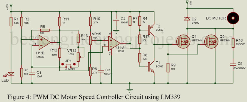
Here, in this circuit, we are using a variable square pulse generator shown in figure 3. The circuit of the DC motor speed controller is shown in figure 4.
The rate at which the PWM pulse is triggered is determined by the Operating Frequency (F) that we just calculated (rising edge of pulse). As a result, the greater the square wave operating frequency, the faster the pulse production process, which ultimately affects the motor speed.
Comparator as a pulse width modulator:
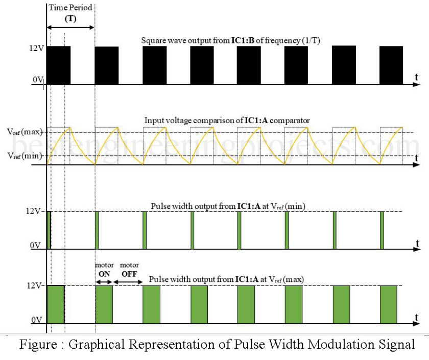
Here we employ a second voltage comparator from the LM339 IC (i.e. IC1:A) as a pulse width modulator. An adjustable reference voltage (Vref) is given to the non-inverting input(+) of the IC1:A comparator using resistors R10, VR15, and R6, as illustrated in Figure 4. In contrast, the output from the preceding comparator (IC1:B) is sent to the inverting input(-). The Pulse Width Modulation method is graphically explained in the following Figure 5. The Vref voltage ranges from around 1.834V to 10.16V, depending on the 12V power supply and voltage divider acting on non-inverting input(+) of the IC1:A. This means that if Vref is close to 10V, the pulse width is near 50%, and if Vref is close to 2V, the pulse width is near 15% of the Time Period. Hence, adjusting the Vref causes Pulse Width Modulation, which in turn determines the motor speed.
Motor Switching Process:
The inverting input(-) of the IC1:A comparator is fed with a square wave signal of the required frequency, generated by IC1:B. The non-inverting input(+) of IC1:A is allocated with a fixed reference voltage. As illustrated in Figure 4, the output of the IC1:A comparator is fed into a combination of two transistors BC557 (PNP) and BC547 (NPN).
As a result, anytime the potential difference (Vd) between the inputs of IC1:A becomes negative, the comparator output changed to a logic LOW, activating the PNP transistor while turning off the NPN transistor. This gives the MOSFETs (i.e.Q1, Q2) enough gate potential, completing the circuit path for motor control. When the potential difference (Vd) between the inputs of IC1:A becomes positive, the comparator output generates logic HIGH, activating the NPN transistor while switching off the PNP transistor. As a result, the MOSFETs (i.e.Q1, Q2) remain turned off, preventing the motor from turning on. In this way, speed control of the DC motor can be achieved with variable frequency and variable PWM method. The Resistor R16 and Capacitor C5 act as snubber circuits and protect the circuit from the back EMF of the motor. LED1 is for power indication.
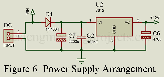
Power Supply Arrangement for PWM DC Motor Speed Controller Circuit:
DC Power supply between 14V and 30V according to the motor power supply is connected to the input pin. This supply is further converted into +12V using a fixed voltage regulator IC for the control circuit.
PCB Diagram
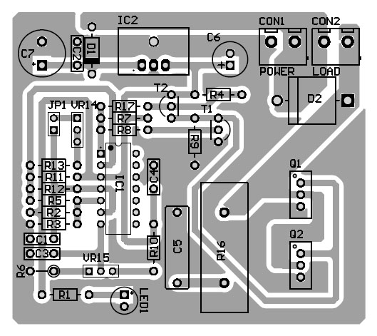
PCB of DC motor speed controller is designed using Altium design software. The solder side and component side are shown in the figures below. You can download the actual size PCB and component side PCB in PDF format from the link below.
Figure 8: Solder Side PCB
CLICK HERE TO DOWNLOAD PCB DIAGRAM IN PDF FORMAT
Components required for PWM DC Motor Speed Controller Circuit
| Resistor (all ¼-watt, ± 1% Carbon Unless Stated Otherwise) |
| R1 = 1.8 KΩ
R2, R3, R5 = 68KΩ R4, R7 = 2KΩ R6, R10 = 2.7KΩ R8, R9, R13, R17 = 10KΩ R11 = 1k R12 = 330k VR14 = 100k (pot) VR15 = 10K (pot) R16 = 15 Ohm(5W) |
| Capacitors |
| C1 = 10nF (Ceramic disc)
C2, C3, C4 = 100nF (Ceramic disc) C5 = 68nF/400V (polymer film capacitors) C6 = 470uF/50V (electrolytic capacitor) C7 = 2200uF/50V (electrolytic capacitor) |
| Semiconductor |
| IC1 = LM339 Quad comparator IC
IC2 = LM7812 (Series fixed voltage regulator) D1 = 1N1004 (Rectifier Diode) D2 = BY500 (High power diode) Q1, Q2 = IRFZ44N (MOSFET) T1 = BC547 (General purpose NPN transistor) T2 = BC557 (General purpose PNP transistor) |
| Miscellaneous |
| LED1 = Any color 5mm LED
Heatsink for voltage regulator and MOSFET Jumper |
