Introduction to Sample-and-Hold Circuit
Most analogs to digital converter (A/D) integrated circuits come with sample and hold circuits (S/H) integrated into the system, but it is still necessary for the user to have a good understanding of its operation, including both the capabilities and the limitations of the Sample and hold circuit.
A typical S/H circuit is shown in Figure 1. The analog signal is typically inputted into a buffer circuit. The purpose of the buffer circuit is to isolate the input signal from the S/H circuit and to provide proper impedance matching as well as drive capability to the hold circuit. Many times the buffer circuit is also used as a current source to charge the hold capacitor. The output of the buffer is fed to an analog switch, which is typically the drain of a JFET, junction field-effect transistor, or a MOSFET, metal-oxide-semiconductor field-effect transistor. The JFET or MOSFET is wired as an analog switch and controlled at the gate by a sample pulse generated by the sample clock. When the JFET’s or MOSFET’s gate is asserted, the switch will short the analog signal from drain to source. This connects the buffered input signal to a hold capacitor. The capacitor begins to charge to the input voltage level at a time constant determined by the hold capacitor’s capacitance and the analog switch’s and buffer circuit’s “on” channel resistance.

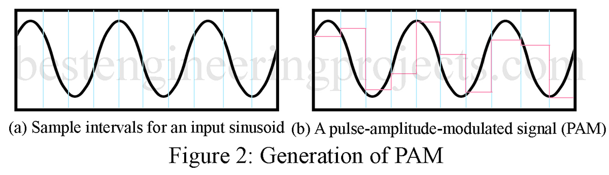
When the analog switch is turned off, the sampled analog signal voltage level is held by the hold capacitor. Figure 2(a) shows a picture of a sinusoid on the input of the S/H circuit. The sample times are indicated by the green vertical lines. In Fig. 2(b) the sinusoid is redrawn as a sampled signal. Note that the sampled signal maintains a fixed voltage level between samples. The region where the voltage level remains relatively constant is called the hold time. The resulting waveform, shown in Fig. 2(b), is called a pulse-amplitude-modulated (PAM) signal. The S/H circuit is designed so that the sampled signal is held long enough to be converted by the A/D circuitry into a binary representation.
The time required for an S/H circuit to complete a sample is based partly on the acquisition and aperture times. The acquisition time is the amount of time it takes for the hold circuit to reach its final value (during this time the analog switch connects the input signal to the hold capacitor). The acquisition time is controlled by the sample pulse. The aperture time is the time that the S/H circuit must hold the sampled voltage. The aperture and acquisition times limit the maximum frequency at which the S/H circuit can accurately process the analog signal.
To provide a good-quality S/H circuit a couple of design considerations must be made. The analog switch “on” resistance must be small. The output impedance of the input buffer must also be small. By keeping the input resistance minimal the overall time constant for sampling the analog signal can be controlled by the selection of an appropriate hold capacitor. Ideally, a low capacitance should be selected so that a fast charging time is possible, but a small capacitor will have trouble holding a charge for a very long period. A 1-nano-farad hold capacitor is a popular choice for many circuit designers. It is also important that the hold capacitor is of high quality. High-quality capacitors have dielectrics of polyethylene, polycarbonate, or Teflon. These types of dielectrics minimize voltage variations due to capacitor characteristics.