Metal Oxide Semiconductor FET (MOSFET)
MOSFET is of greater commercial importance than the junction FET.
Types of MOSFET
- Enhancement MOSFETs and
- Depletion MOSFETs.
Enhancement Type MOSFET
Figure 1 gives the cross-sectional view of a p-channel enhancement MOSFET. It consists of a lightly doped n-type substrate into which all diffused two highly dipped p + region spaced 10 to 20um apart. One region, say the left-hand region, acts as the source while the other region acts as the drain. A thin insulating layer of SiO2 of thickness 1000 to 2000 A is grown over the entire surface of the device. Holes are cut into the SiO2 layer and aluminum contacts are made to p+ source and drain regions. Subsequently aluminum layer is formed over the entire SiO2 layer covering the entire channel from source to drain.
This aluminum forms the gate. Metal contacts are made to the source, drain and get regions as shown in figure 1. The chip area is extremely small, being only about 5 sq. mils. This area is about 5% of that required for BJT.
You can checkout other article related to MOSFET
The metallic gate layer and the semiconductor channel from a parallel plate capacitor with SiO2 as the dielectric in between. The gate Layer has been insulated from the rest of the device by means of SiO2 layer. Hence, the device is called insulated gate FET. The SiO2 layer results in an extremely high input impedance of the MOSFET lying in the range 1010 to 1015 ohms.
Now let us ground the substrate and apply a negative voltage at the gate. This results in an electric field normal to the SiO2 layer. This electric field terminates on induced positive charges in the semiconductor material between source and drain at the sites shown in figure 1. These positive charges from minority carrier in the n-type substrate and result in an inversion layer in the region between source and drain.
As the magnitude of the negative voltage at the gate is increased, the concentration of induced positive charges in the semiconductor increases. This in turn increases the conductivity of the region just below SiO2 layer and increases the current from source to drain. Thus, increased negative voltage at the gate increases or enhances the drain current and this MOSFET is, therefore, called enhancement MOSFET.
Static Characteristic Curves | MOSFET
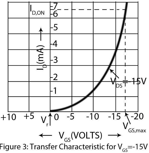
Figure 2 gives the static drain current versus drain voltage characteristic of a typical p-channel enhancement MOSFET, using VGS as the parameter. Figure 3 gives a transfer characteristic for VDS = -15 volts for the same device. Figure 2 shows that the drain characteristic of enhancement MOSFET are similar to those of junction FET. Transfer characteristic of figure 3 shows that the saturation current is extremely small, of the order of a few nano-amperes for VGS = 0 or positive. But as VGS is made more and more negative, the magnitude of drain current first increases slowly and then relatively fast with increases of |VGS| beyond a few volts.
Current ID,ON This is the maximum permitted drain current. Manufacturer’s data gives ID,ON and also the voltage VGS needed to get ID,ON.
Gate-source Threshold Voltage VGST or VT It is the value of VGS at which drain current |ID| reaches some prescribed small value typically chosen as 10 uA. For a p-channel MOSFET, typical value of Vt is -4 volts and the corresponding value of drain supply voltage VDD is -12 volts.
Depletion Type MOSFET | Types of MOSFET
Figure 4 shows the basic structure of n-channel depletion MOSFET. If consists of a lightly doped p-type substrate into which two highly doped n+ regions are diffused forming the source and the drain. An n-channel is diffused between the source and the drain. Similar to enhancement MOSFET, a thin layer of SiO2 layer if formed allowing contacts with the source and the drain. Finally, gate metal area is overlaid the oxide layer covering the entire channel. Metal contact are made into the source, drain and gate.
In delectation layer MOSFET, unlike enhancement MOSFET, an appreciable drain current IDSS (Saturation drain current with VGS = 0) flows. With negative gate voltage, positive charge gets induced in the n-channel through SiO2 layer of the gate capacitor as shown in figure 5. In an n-channel FET, drain current is due to majority carrier electrons. These induced positive charges in the channel region result in delectation of majority carrier electrons in the channel as shown in figure 5 and hence make the n-channel less conductive. Because of the depletion of majority carriers in the channel, this MOSFET is called delectation MOSFET. As the gate voltage is made and mode negative, the drain current corresponding reduces.
The voltage drops in the channel due to drain current flow results in the channel region nearest to the drain to be more depleted than the region close to the source as shown in figure 5. This condition is similar to the pinch off phenomenon in JFET. Hence the volt-ampere characteristic of the depletion MOSFET are similar to those of JFET.
Drain and Transfer Characteristics
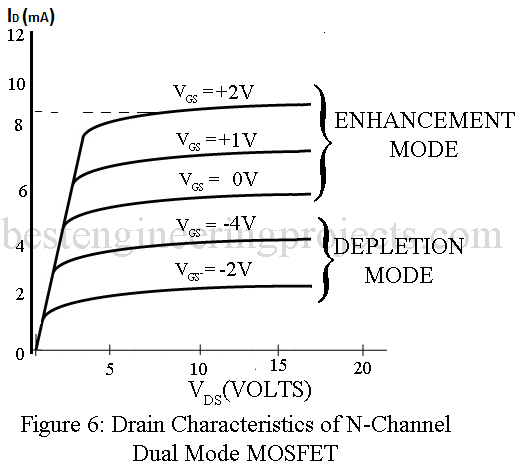
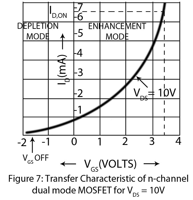
Figure 6 shows the drain current versus drain voltage characteristic of this MOSFET for both depletion mode (negative gate voltage VGS) and enhancement mode (positive gate voltage VGS). Figure 7 gives the transfer characteristic for VDS = 10 volts for both enhancement mode and depletion mode. Since the operation is possible for both the modes, this MOSFET may be called dual mode MOSFET.
Gate Source Cutoff Voltage. VGS,OFF For a specified VDS, VGS,OFF is the gate-source voltage at which ID reduces to a certain specified negligibly small value as shown in figure 7. This voltage VGS,OFF corresponds to the pinch off the voltage VP of JFET. Figure 7 also shows the maximum permitted drain current ID,ON.
Gate Protection in MOSFETs
On application of large gate voltages, an open circuit gate may accumulate enough charge so as to produce an electric field large enough to puncture the extremely thin SiO2 layer. To eliminate this possibility, we may fabricate a zener diode between gate and substrate. With normal operating voltages, the zener diode remains open and does not influence the working of the circuit. In case of an extremely high gate voltage, the zener diode breaks down thereby limiting the gate potential to a value equal to the zener diode breakdown voltage.
Circuit Symbol and Small Signal Model of MOSFETs
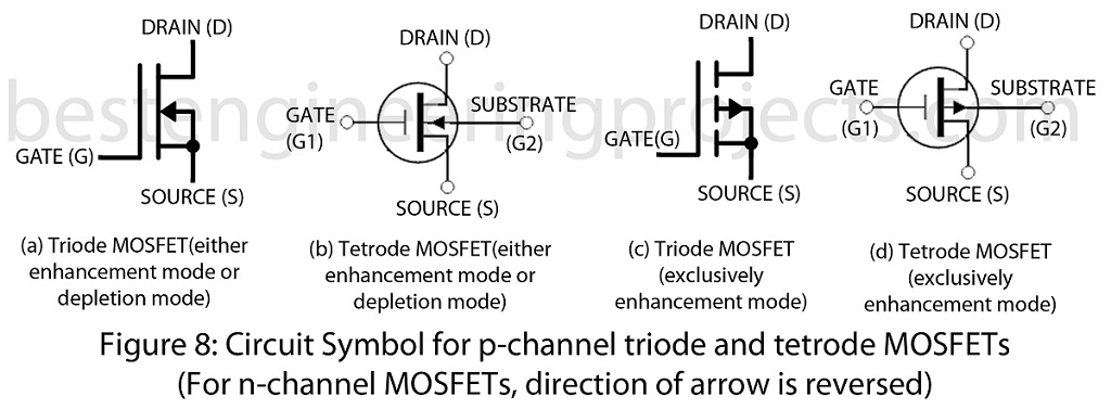
- Symbol Basically a MOSFET is a triode with the substrate internally connected to the source. Figure 8(a) gives the circuit symbol for p-channel triode MOSFET (applicable to both enhancement type and delectation type). Figure 8(b) gives the circuit symbol for p-channel tetrode MOSFET (Applicable to both the enhancement type and depletion type). Here a separate connection has been brought out for the substrate. Figure 8 (c) gives circuit symbol for a p-channel triode MOSFET exclusively of enhancement type. For a n-channel MOSFET, direction of arrow in circuit symbol is reversed.
- Small Signal Models The low frequency small signal model for MOSFT between terminals (G(=G1)), S and D is the same as shown in figure in previous article (), for JFET provided that the substrate has been connected to the source. Small resistances of the source and the drain have been neglected in the model. The value of gm for MOSFET is comparable with that of JFET (being 0.1 to 20 mS). However, as seen from Table 1, the input resistance rgs and feedback resistance rgd of MOSFET are much greater than those of JFET while the value of drain resistance rd of MOSFET is much smaller than that of JFET.
In case, the substrate terminal G2 is not connected to the source, the MOSFET model of figure in previous article has to be modified as below:
- A diode D1 representing the pn junction between the substrate and the source should be connected between the terminal G2 and S.
- Another diode D2 representation the PN junction between the substrate and the drain should be connected between terminals G2 and D.


