Mobile phones and small electronic gadgets are powered by AC mains using an AC adapter. In the event of mains failure, a low-capacity UPS will do the job satisfactorily. Here we design a simple, efficient, economical, and easy-to-construct UPS for mobile phone or telephone sets. The project advanced mini-UPS circuit can also be used for high power by changing a transformer with a high current rating so this circuit can be used as power backup for laptops also. We have already posted 350VA Offline UPS Circuit.
Block Diagram of Advance Mini UPS
The block diagram of the circuit advance mini UPS with charger unit is shown in figure 1. Normally, small power electronic gadgets utilize a current of less than 500mA to enable the circuit and to charge the battery. It consists of a power supply for electronic gadgets, charger unit, switching unit, SC sensor, etc. The output power of 5 watts is delivered by the circuit advance mini UPS which is sufficient for most small powered gadgets.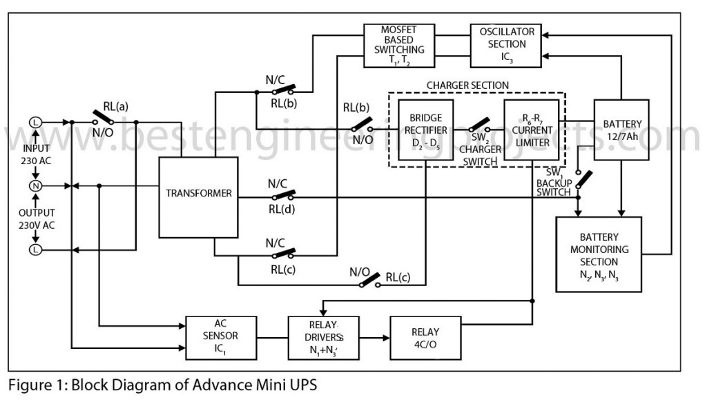
Description of Advance Mini UPS Circuit
The circuit diagram of the advanced mini UPS is shown in Figure 2. IC1 is an optocoupler IC and consists of an LED and a phototransistor which is used here as an AC sensor. When AC mains are available internal LED of IC1 glows which activates the internal phototransistor. As a result, the output of IC1 becomes high which is connected to the input of gate N1 of IC2 as well as a 12V SMF battery. When the output of IC1 is high, the output of gate N1 of pin 3 also goes high and relay RL1 energizes via relay driver transistor T3.
When relay RL1 energizes it conducts mains AC supply to the primary of the transformer X1 and is also available at the output of UPS. Transformer X1 stepped down the input AC mains voltage to 9V-0-9V which is further rectified by using diode D2 through D5. The availability of secondary voltage is indicated by glowing LED1 which is connected to the secondary coil of transformer X1 through resistor R3. The battery is charged through the charger circuit provided charger switch SW2 is ‘on’ (closed). The power supply to IC3 through relay contact RL1 (d) is disconnected. As a result, the transformer works as a charger transformer and the battery starts charging through current-limiting resistors R6 and R7.

When switch SW1 is in on position and AC mains supply fails it de-energizes the relay RL1 instantly and as a result, the circuit is used in inverter mode.
Check out other power supply and inverter circuits posted on besengineeringprojeccts.com
- Offline UPS Circuit
- Advance Emergency Light Circuit
- 3000W Inverter with Inbuilt Charger using AT89C2051
- Crystal-controlled inverter | Verified Inverter Circuit
Inverter Section | Advance Mini UPS Circuit
The inverter circuit is wired around IC3 an astable multivibrator mode operating at a frequency of 50 Hz. The output from pin 10 and pin 11 of IC3 directly drives the MOSFET transistors T1 and T2. These two MOSFETs (T1 and T2) are configured in push-pull mode. Capacitor C1 is used to filter DC signals if any available at the output of the inverter circuit.
At the time when the battery voltage becomes less than 10V, the output of gate N2 at pin 4 goes high which further fires the SCR1 through resistor R17. As a result, the supply voltage is pulled down to the ground via RL1 (d), diode D8, resistor R12, and SCR1 which disable the oscillator due to the absence of the power supply of IC3. Glowing LED5 indicates the battery is out of use i.e. cut-off condition. When the battery voltage is less than 13.5V or more than 10V the output of gate N2 at pin 4 becomes low and as a result, SCR1 does not fire. Glowing LED4 indicates that the battery is ready for use.
PCB Design | Advance Mini UPS Circuit
The actual-size, single-side PCB layout for the circuit of advanced mini UPS is shown in Fig. 3, and the layout of its components in Fig. 4.

Figure 3: Actual Size Solder Side PCB Design for Advance Mini UPS
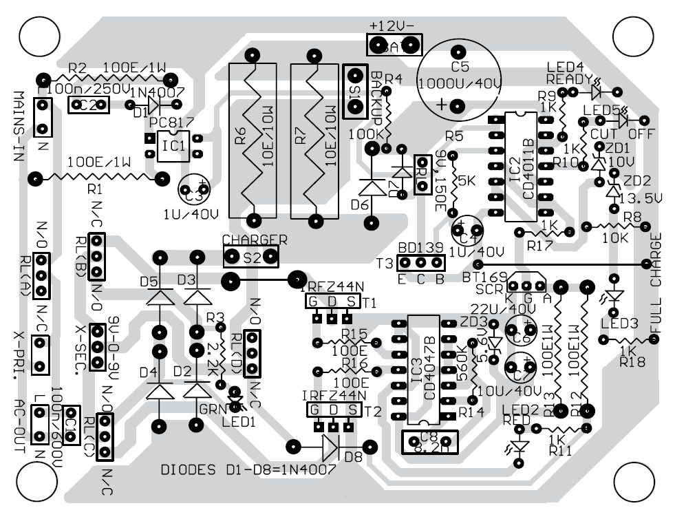
Figure 4: Component Side PCB Design for Advance Mini UPS
The proposed front-panel layout for the advanced mini UPS, including LED arrangement, is shown in Fig. 5.

PARTS LIST OF ADVANCE MINI UPS CIRCUIT
|
Resistor (all ¼-watt, ± 5% Carbon) |
|
R1, R2, R12, R13 = 100 Ω, 1 WATT R3 = 2.2 KΩ R4 = 100 KΩ R5 = 5 KΩ R6, R7 = 10Ω, 10 WATT R8 = 10 KΩ R9, R10, R11, R17, R18 = 1 KΩ R14 = 560 KΩ R15, R16 = 100 Ω |
| Capacitors |
| C1 = 100nF, 600V (Polyester Capacitor)
C2 = 100nF, 250V (Polyester Capacitor) C3, C4 = 1 µF, 40V (electrolytic capacitor) C5 = 1000 µF, 40V (electrolytic capacitor) C6 = 22 µF, 40V (electrolytic capacitor) C7 = 10 µF, 40V (electrolytic capacitor) C8 = 8.2nF (ceramic disc) |
| Semiconductors |
|
IC1 = PC817 (optocoupler) IC2 = CD4011B (Quadruple 2-input NAND gate) IC3 = CD4047 (mono/astable multivibrator) SCR1 = BT169 T1, T2 = IRFZ44N (N-channel MOSFET) T3 = BD139 (NPN transistor) D1 – D8 = 1N4007 (rectifier diode) ZD1 = 10V (zener diode) ZD2 = 13.5V (zener diode) ZD3 = 5.6V (zener diode) LED1, LED4 = Green LED LED2, LED3, LED5 = Red LED |
| Miscellaneous |
| X1 = 230V AC primary to 9V-0-9V, 2A secondary transformer
RL1 = 9V, 150Ω 4C/O relay SW1, SW2 = SPST switch B1 = 12V, 7Ah SMS battery |
sir, i need the pcb design of 800 va ups which can give 1 hour current backup for a desktop computer. please help me by providing it.
Hi, i just want to thank you for this circuit diagram and PCB design, and i am just curious why is there switch for battery charger can you add auto charger to be complete UPS or is that already auto charger via that 4011 IC do i need to switch off charger when battery is fully charged and do i need to switch it off when there is no power coming from mains outlet.
For automatic charging the link given below will help you
http://bestengineeringprojects.com/12v-7ah-smart-battery-charger-with-pcb-diagram/
http://bestengineeringprojects.com/12-v-battery-charger-with-overcharge-and-deep-discharge-protecting/
and for automatic changeover changeover unit the link given below will help.
http://bestengineeringprojects.com/offline-ups-circuit/
Thank you for quick reply i will try this.
We will use this circuit for our power electronics thank you so much for this circuit. May we ask why the two ICs here in Philippines did not suite the IC in the design? Or maybe can we request for the softcopy of the design? Thanks
Why is Ic 2 fire
Not working project please help