In class B push pull amplifier, output current (collector current) flows for only half the cycle of the input signal. Hence distortion is excessive. Single ended operation is, therefore, not possible in class B audio amplifier. Class B audio (un-tuned) amplifier must necessarily use push pull operation to reduce distortion. In effect, in class B push pull amplifier, one transistor say Q1 conduct during one half cycle while the other transistor namely Q2 conducts during the other half cycle.
Class A power amplifiers may use either single ended or push pull operations. However, in most class A power amplifier, push pull operation is preferred because of the various merits mentioned above.
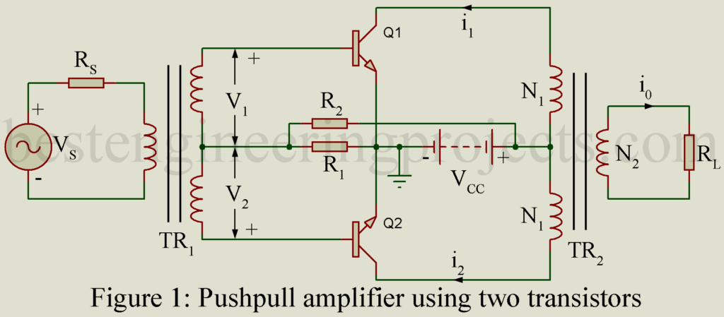
The circuit of class B push pull amplifier is the same as that of class A push pull amplifier. The difference lies in the order of biasing. In class B circuit, the transistor are biased approximately to cutoff. Hence the circuit of figure 1 represents class B push pull amplifier also if resistor R1 is made zero because a silicon transistor is basically at cutoff if its base is short circuited to emitter.
Advantage of Class B Push pull Amplifier over class A Push pull Amplifier
- Greater power output
- Higher conversion efficiency
- Negligible power loss with zero signal
Because of zero power drainage with zero signal, in amplifiers using solar cell or simple batteries, class B operation is preferred.
Drawbacks of class B Pushpull Amplifier
- Harmonic distortion is higher
- Self-biased not be used
- Supply voltage is required to have good regulation
Collector Circuit Efficiency | Class B Push Pull Amplifier
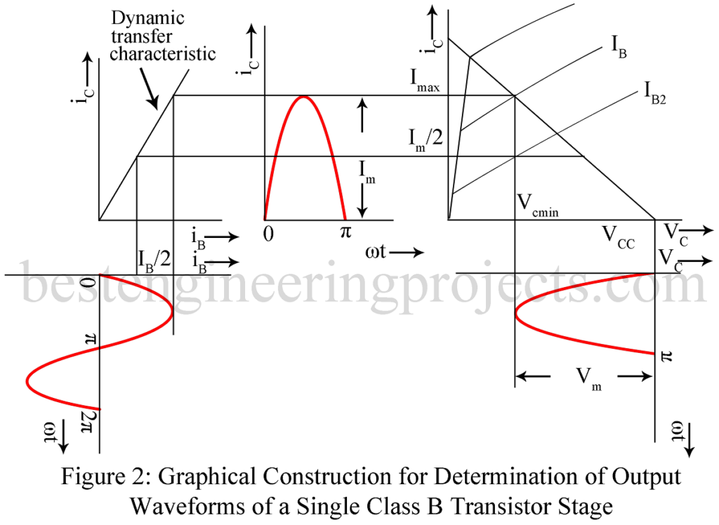
We assume that the transistor characteristics are linear, parallel and equi-spaced for equal increments of excitation so that the dynamic transfer characteristics is a straight line as shown in figure 2. We also assume that the minimum current is zero. Figure 2 demonstrates the graphical method of determination of collector current and collector voltage wave shaped for a single transistor say transistor Q1 operating under class B condition.
With sinusoidal excitation base current iB, the collector current iC and the collector voltage vC are also sinusoidal during one-half of the a.c. cycle and zero during the other half. The effective load resistance RL1 for one transistor is  where RL is the load resistance across the secondary of the output transformer TR2, N1 is the number of turns on one-half of the primary and N2 is the number of turns on the secondary as shown in figure 1.
Waveform of ic and vc corresponding to transistor Q1 alone. Waveform of transistor Q2 are similar to those shown in figure 2 but 1800 out of phase. Hence the load current in the secondary being proportional to the difference of the two collector currents, forms a perfect sine wave.
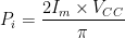
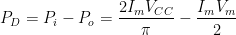
Power output ![P_o = \dfrac{I_m\times V_m}{2} = \dfrac{I_m}{2}[V_{CC}-V_{min}]](https://s0.wp.com/latex.php?latex=P_o+%3D+%5Cdfrac%7BI_m%5Ctimes+V_m%7D%7B2%7D+%3D+%5Cdfrac%7BI_m%7D%7B2%7D%5BV_%7BCC%7D-V_%7Bmin%7D%5D&bg=ffffff&fg=000&s=0&c=20201002) …….(1)
…….(1)
D.C. load line in each transistor under loaded condition is the average value of the half sine wave of ic of figure 2. Hence for this half sine wave,
 ……(2)
……(2)
Hence the dc power input to both the transistors form the collector supply is,
 …….(3)
Hence collector circuit efficiency is,
 …..(4)
 ……(5)
……(5)
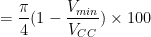
Equation 5 shows that the maximum possible value of collector circuit efficiency for class B amplifier is  i.e. 78.5%. This maximum theoretical value is higher than the corresponding value of 50% for class A transformer coupled amplifier.
For such transistor circuit where Vmin << VCC, collector circuit efficiency closely approaches the theoretical maximum limit. Basically, this high value of collector circuit efficiency in class B amplifier becomes possible because of the fact that in class B amplifier, current is zero with zero excitation whereas in class A amplifier, there is drain from VCC source even at zero signal. It is worth nothing that in a class B amplifier, collector dissipation is zero signal and increases with increase of signal magnitude while in a class A amplifier, collector dissipation is maximum with zero signal and decreases with increases of signal magnitude.
In class B amplifier, the d.c. component of collector current increase with increase of signal. Hence power supply regulation must be good.
Collector Dissipation of Class B Push Pull Amplifier
Total collector dissipation PD in both transistors is equal to the dc power input from collector supply voltage minus the power delivered to the load. Hence,
 ……(6)
……(6)
But  …….(7)
Hence  ……..(8)
With zero excitation, Vm = 0. Hence, as per equation 8, collector dissipation is zero with zero excitation. Using equation 8, it may be shown that the collector dissipation increases with increase of excitation and passes through a maximum at  .
.
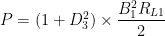
Hence maximum collector dissipation PD, max is obtained from Equation 8 on putting . ……(9)
Thus,  ……..(10)
Maximum Power Output of Class B Push Pull Amplifier
Maximum output power is obtained when Vm = VCC i.e. when Vmin = 0. Hence,
 …….(11)
From equation (10) and (11) we find that,
 ……(12)
From equation (12) we conclude that the two transistors of a class B amplifier taken together must be able to dissipate about 40% of the maximum power output. For a class AB amplifier designed to deliver maximum power output of say 50 watts, PDmax – 20 watts i.e. each transistor must be capable of dissipating 10 watts. Hence, we conclude that class B pushpull amplifier is capable of providing output power 5 times the power dissipation capability of each transistor.
On the other hand, in class A amplifier using parallel operation of two transistor to get the same output power of 50 watts, assuming maximum conversion efficiency of 50%, dc power requirement is 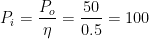 watts. This complete power of 100 watts must be dissipated in the two transistors are zero signal. Thus, each transistor must be capable of dissipating 50 watts. Thus, with zero excitation, in class A operation there is a steady loss of 50 watts in each transistor whereas in class B amplifier the standby or zero excitation collector dissipation is zero. This clearly establishes the superiority of class B push pull operation over class A parallel operation.
Distortion in Class B Push Pull Amplifier
In a push pull amplifier, even harmonic get eliminated from the output. Then the only harmonic distortion of significance is the hard-harmonic distortion. Thus, is given by,
 …….(13)
Power output, taken distortion into account, is given by,
 …….(14)
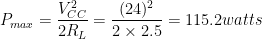
Example 1 The idealized pushpull class B power amplifier shown in figure 1 has R2 = 0, VCC = 24 volts, N2 = 2N1 and RL = 10 -ohm. The transistors have hfe = 30. Input is sinusoidal. For the maximum output signal at Vm = VCC, determine (a) the output signal power (b) the collector dissipation in each transistor. Also calculator the maximum collector dissipation per transistor.
Solution: 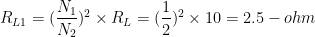
When Vm = VCC, power output is
Total collector dissipation in the two transistors is,

At  ,
,
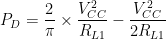


Hence dissipated in each transistor = 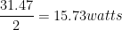

Hence maximum collector dissipation per transistor 
Can u help me with this
Anidealclass Bpushpullpoweramplifierwithinput andoutput transformers have Vcc=20V, N2=2N1and RL=20Ω. The transistors have hfe=20. L et input be sinusoidal.
Forthe maximumoutput signalat VCE(p)=Vcc. Determine i) the output signalpower ii)thecollectordissipationineachtransistoriii)theconversionefficiency.
Wonderful explanation