The protection of electrical and electronic appliances is the main concern these days. Some electronics appliance is very sensitive to voltage i.e. it only functions when adequate voltage is provided. Some appliances were even destroyed due to high and low voltage supply. To solve this type of issue we are posting a very simpler and more useful project called “High Low Voltage Cutout Circuit”. Previously we had already posted various types of appliance protecting circuits on bestengineeringprojects.com like:
- Auto Cut Circuit for Over and Under Voltage
- High Current Regulator Circuit
- AC Voltage Stabilizer Circuit using 556
- Overvoltage Protection Circuit
- Automatic Voltage Stabilizer Circuit
The difference is, that this circuit is simple and more sensitive than the previous one.
Circuit Description of High Low Voltage Cutout Circuit
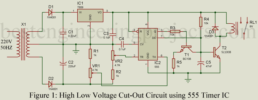
The circuit of high-low voltage cutout is shown in Figure 1. The main building block of this circuit is timer IC 555, voltage regulator IC and a few other activities as well as passive electronic components like a transistor, resistor, capacitor, etc. For a better description, we divide the entire circuit into three different reasons.
-
Voltage Step-Down and Rectifier Unit | High Low Voltage Cutout Circuit
This unit is a rectifier unit. The mains input is stepped down to 12V-0V-12V using the center tap transformer which is further rectified using diodes D1 and D2 (Full wave center tap rectifier). The rectified output is pulsating in nature and needs to filter. Here we have used two capacitors C1 and C2 to smoothen the waveform. One-half of rectified output is given to 9V fixed series voltage regulator IC (IC1) where the other half is left for reference.
Reference Circuit | High Low Voltage Cutout Circuit
This unit is built around voltage-regulated IC and timer IC. The output from diode D1 is given to the voltage regulator IC, thus output is fixed whereas the output of diode D2 is fluctuating. This fluctuating voltage (output of diode D2) is proportional to fluctuating in mains input. When the mains voltage becomes higher than normal, the voltage at pin 6 of timer IC 555 (IC2) also becomes high. This high voltage at pin 6 drives the output at pin 3 of IC2 high. Similarly, when the voltage becomes lower than the voltage at pin 2 of the timer IC becomes low, and pin 7 is also grounded.
Switching Circuit | High Low Voltage Cutout Circuit
The switching circuit is designed around two general-purpose transistors (T1 = BC108C, T2 = SL100B). In either case (i.e. low and high voltage) the transistor T2 becomes off as a result relay RL1 is de-energized.
Case I: When voltage is high
When the mains voltage becomes high than the normal voltage, the voltage at pin 6 also becomes high. Thus, the output of IC2 (NE555) becomes high, transistor T1 starts to conduct, and the base of transistor T2 is grounded. This led transistor T2 to off state and the relay was de-energized.
Case II: When voltage is low
When the mains voltage becomes low, the voltage at pin 2 of IC2 (Timer IC 555) also becomes low, and pin 7 will be grounded. Thus, the base of transistor T2 is again grounded and the relay drives to de-energized.
Case III: When voltage is normal
The output of the voltage regulator and output from diode D2 become equivalent as a result neither out of IC2 become high nor pin 7 of IC2 will be grounded. Thus, the base of the transistor gets enough voltage to conduct and the relay is energized.
PCB Diagram:
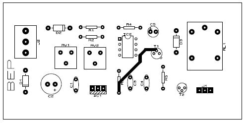
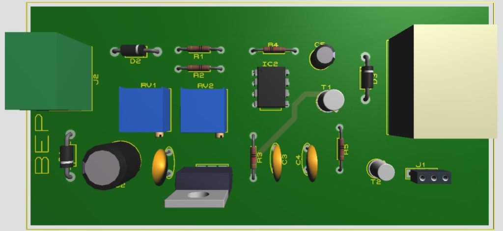
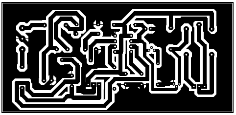
The PCB diagram is designed using Proteus 8.1 design suite. The actual size solder side and component side are shown in the figure below. Download the PCB diagram in PDF format from the link given below.
Figure 2: Solder side PCB of High Low Voltage Cutout


Click here to download the PCB
PARTS LIST OF HIGH LOW VOLTAGE CUTOUT CIRCUIT
| Resistors (all ¼-watt, ± 5% Carbon else Specified) |
| R1, R2, R5 = 1 KΩ
R3, R5 = 10 KΩ |
| Capacitors |
| C1 = 0.22 µF (Ceramic Disc)
C2 = 220 µF, 25V (Electrolytic Capacitor) C3, C4 = 0.1 µF (Ceramic Disc) C5 = 47 µF, 16V (Electrolytic Capacitor) |
| Semiconductors |
| IC1 = NE555 (Timer IC)
IC2 = LM7809 (9V Series fixed voltage regulator) T1 = BC108C (General purpose NPN transistor) T2 = SL100B (General purpose NPN transistor) D1 – D3 = 1N4001 (Rectifier Diode) |
| Miscellaneous |
| X1 = 220V AC Primary, 12V-0V-12V, 500 mA secondary, center tapped transformer
RL1 = 9V, 200Ω relay |


do it work??????????