Large Signal Amplifier | Power Amplifier: In a multistage amplifier, first stage or the input stage and the intermediate stage are usually small signal class A amplifier stage while the last stage (the output stage) or sometimes last two stage are large signal amplifier (power amplifier) stage. Small signal amplifier stages serve to amplify the weak input signal to a sufficient large value to drive the final stage. The output stage generally feeds a transducer such as CR Tube, a loud speaker, a servo-control motor etc. the large signal amplifier stage must be capable of handling large voltage or current swing and hence capable of delivering large power to the load.
As we had discussed in previous article, analysis of a small signal amplifier is usually done by replacing the amplifying device i.e. BJT or FET by its small signal a.c. model. Alternatively, we may resort to graphical analysis. However, the first method is more easy and popular. In the analysis of large signal amplifier stage, on the other hand, we cannot use small signal a.c. model for BJT or FET since output voltage and current swing are very large, much beyond the linear range of the dynamic characteristics.
Hence in the case of large signal amplifier, we must necessarily resort to graphical analysis utilizing the output characteristics of the amplifying device namely BJT or FET. Large output current and voltage swing beyond the linear region result in harmonic distortion in large signal amplifier can be kept within limits.
Important quantities in the study of large signal amplifiers are: distortion, output power, conversion efficiency, bias stabilization and tendency of thermal runway.
Large signal untuned amplifier may be operated under class A, AB or B conditions but never under class C configuration. As we move from class A TO Ab, B and C operation, conversion efficiency increases but distortion also increases. In class C operation of untuned amplifier, distortion is excessive. Hence class C untuned amplifiers are never used. We here study the large signal untuned amplifiers of class A, AB and B types.
Class A Large Signal Amplifiers or Power Amplifier
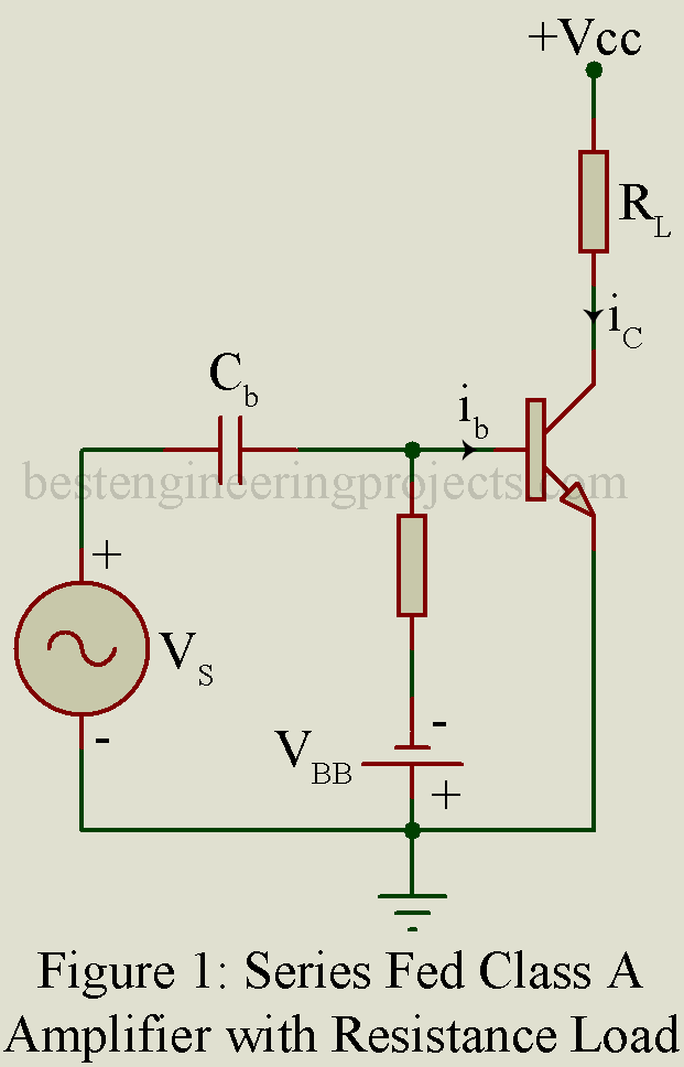
Figure 1 gives the schematic circuit of a series fed class A CE amplifier stage using resistive load RL. As per standard notation, iB, ib and Ib represent respectively the total instantaneous base current, instantaneous time varying base current and quiescent (zero signal) base current. Similarly, iC, ic and VC represent respectively the total instantaneous, instantaneous time carrying and quiescent values of collector voltage.
We assume here that the static output characteristics of BJT are equidistance for equal increments ib of the input base current. Then for sinusoidal as shown in figure 2. This forms the ideal condition and the nonlinear distortion is negligible. Power output may take be found graphically.
This a.c. output power is given by,
 …..(1)
Where Vc and Ic are the rms value of the collector voltage and collector current respectively.
Magnitudes of Vc and Ic may be found graphically in terms of maximum and minimum values of output voltage and current as shown in figure 2. For this purpose, we draw from point VCC on the voltage axis, the load line having slope corresponding to the load resistance RL. then intersecting of this load line within bias base current IB gives the quiescent operating point P. let the input signal i.e. the base current varies between the limits IB1 and IB2 i.e. between points P1 and P2 on the load line as shown in figure 2. We project the base current curve on the voltage and current axes to get the waveforms of collector voltage and collector current as shown.
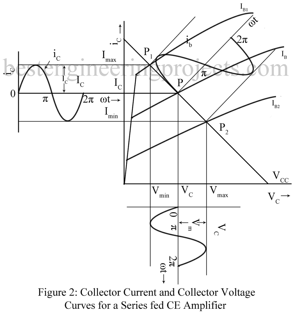
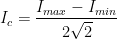
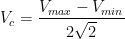
In figure 2, let Im and Vm represent respectively the peak values of sinusoidal collector current and collector voltage. Then rms values are given by,
 …..(2)
And
 …..(3)
Hence the a.c. power output is,
 ……(4)
……(4)
Alternatively, from equation 2 and 3 we get,
 (5)
(5)
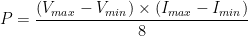
Equation 5 permits us to calculate a.c. output power graphically. Thus we may simply draw the load line on the output characteristics and read the value of 
Example 1 A class A series fed CE amplifier uses resistive load. For a given sinusoidal input signal, the maximum and minimum values of collector current are 12mA and 4mA while the maximum and minimum values of collector voltage are 7.8 volt and 4.2 volt. Calculate (i) the rms values of collector current and collector voltage and (ii) a.c. power output.
Solution:
RMS collector current

RMS collector Voltage

Hence a.c. power output

Question for practice
A class A series fed CE amplifier uses resistive load 4k. For given sinusoidal input signal, the maximum and minimum values of collector current are 15mA and 5mA respectively. Calculate (i) rms collector current (ii) rms collector voltage and (iii) a.c. power output.
Assume linear operation.
[Ans: 3.535 mA; 14.14 volts; 50 mW]