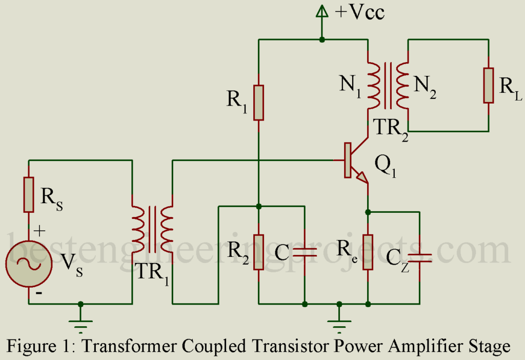
Transformer Coupled Audio Power Amplifier:
Untuned large signal amplifier (power amplifier) of class AB and B type invariably use transformer coupled stages while those of class A type also generally use transformer coupled stage. RC coupled stages are not used because the quiescent current flawing through the load resistor results in large wastage of dc power in it.
This dc power dissipated in the load resistor does not contribute to the useful ac output power. Further flow of dc current through the output device is not desirable. Hence it is preferred to couple the load impedance to the amplifier output circuit through a transformer. Further the input circuit of the transformer coupled amplifier also preferably uses a transformer. Alternatively, the input signal to the transformer coupled power amplifier stage may be fed through RC coupling. Figure 1 gives the basic circuit of power amplifier stage using transformers both in the output circuit and the input circuit.
Impedance Matching | Transformer Coupled Audio Power Amplifier
If a load impedance such as a loud speaker is used, then for maximum transfer of power from the amplifier having high output impedance to the low impedance of 5 to 15-ohm of the voice coil of the loudspeaker, it is required to use step down output transformer. Then for proper impedance match, for an ideal output transformer,
 ……(1)
……(1)
 ……..(2)
Where V1 (V2) is the primary (secondary) voltage, I1 (I2) is the primary (secondary) current and N1 (N2) is the number of primary (secondary) turns.
Turns ratio  . For impedance match, we keep N2 < N1, i.e. n < 1 then the output transformer reduces the voltage in proportion to the turn ratio n. Simultaneously the current gets increase in the same ratio.
From Equation (1) and (2) we get,  …….(3)
But  is the effective input resistance RL1 while
  is the load resistance RL. Then,
 …….(4)
Maximum Power Output | Transformer Coupled Audio Power Amplifier
For getting maximum power output with distortion within specified limits, we are required to choose proper value of ratio n. Generally, the problem is solved graphically. The fest step is to select proper quiescent operating point such that the maximum values of PD, IC and VC are not exceeded during the operation. Quiescent collector current is  where PD is the maximum value of collector dissipation as specified by the manufacturer and VC is that value of quiescent collector voltage which locates the quiescent operating point P near the center of the VCE scale. Considerations involved in the selection of VC are, however, not rigid. The only requirement is that VCE does not exceed VC(max) even when the transistor is driven to cutoff.
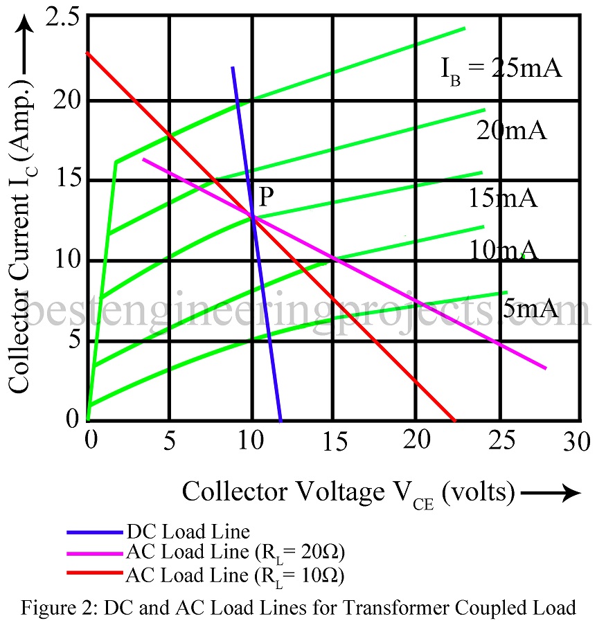
Figure 2 gives the collector current versus collector voltage characteristics of a CE transistor and the dc and ac load lines. For the transistor, let the manufacturer specify PD = 10 watts and VCE,max = 25 volts. Then a properly selected quiescent operating point P is at VC = 10 volts and IC = 1.2 Amp. DC load line is the one passing through this point P with sloe corresponding to the small dc resistance of the transformer primary plus the small emitter circuit – resistor Re as shown in figure 2. Intersection of this load line with the voltage axis gives the required collector supply voltage VCC.
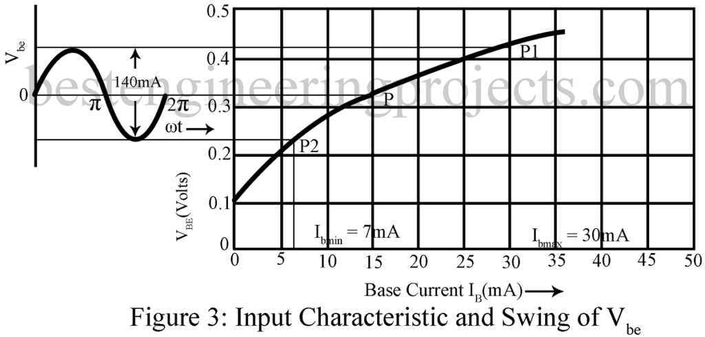
At the quiescent operating point P, the base current is found to be 15mA. If the transistor is driven too close to cutoff, large distortion results. Hence the peak-to-peak voltage swing of base-to-emitter voltage Vbe is restricted to 140 mV. It is assumed here that the input transformer TR1 in figure 1 represents the voltage drive to the power transistor Q and the source resistance RS reflected to the secondary side of the input transformer TR1 is negligible. Figure 3 gives the input characteristic of the power transistor Q.
From this characteristic we find that for this swing of 140 mV in VBE about the quiescent operating point P, the extreme values of base current are Ibmax = 30 mA and Ibmin = 7 mA. We find that although VBE swing is symmetrical, the input base current swing is non-symmetrical about the quiescent base current IB = 15 mA. This non-symmetrical base current swing in fact compensates for the non-symmetrical collector voltage swing. As a result, we have less distortion with voltage drive than with current drive.
In figure 2 several a.c. load lines may be drawn through the quiescent operating point P for different values of RL1. Figure 2 shows two such load lines for values of RL1 equal to 10-ohm and 20-ohm. Subsequently combining a given load line of figure 2 and the input characteristics of figure 3 we construct the corresponding dynamic transfer characteristic plotting collector current iC against base current iB and the output power at fundamental frequency is calculated using equation
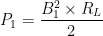
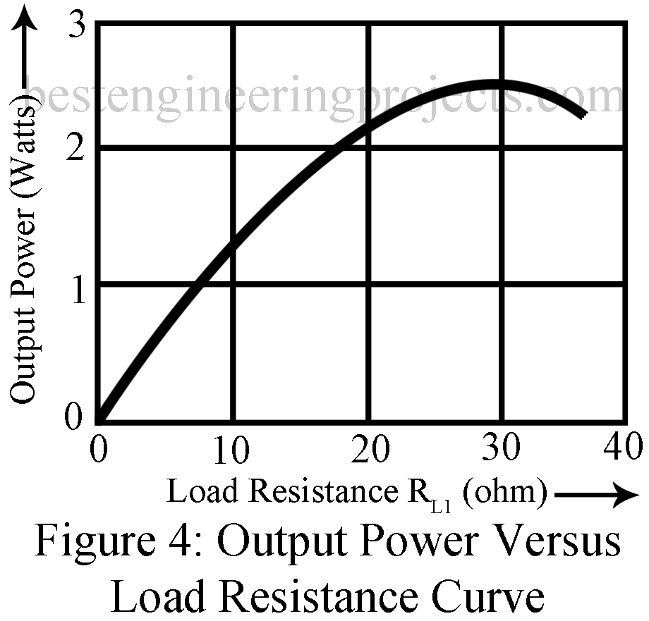
Process is repeated for different load lines of figure 2. We then plot the output power P1 at fundamental frequency against effective load resistance RL1 as shown in figure 4. Subsequently percent second, third and higher distortions are calculated for each value of RL1 i.e. for each load line of figure 2 using any of the methods for calculating distortions and are plotted against RL1 as shown in figure 5. Total harmonic distortion calculated using equation

Is plotted against load resistance RL1.
From figure 4 we find that output power
- Is extremely small for very small value of RL1
- Increases rapidly with increase of RL1 up-to value of RL1 equal to 10-ohm.
- Increases gradually for higher values of RL1 reaching a maximum of about 2.5 watts at RL1 of about 35-ohm and
- Then decreases with further increases of RL1.
The maximum is, however, quite broad.
From figure 5 we find that the distortion is minimum for RL1 of about 10-ohm and increases quite rapidly for higher value of RL1. On using RL1 = 15-ohm, total distortion is less than 10% and the a.c. output power is over 2 watts. On increasing RL1 to about 35-ohm, the output power increases to a high value of 25%. Hence in most cases, a value of RL1 in the vicinity of about 15-ohm is selected. Having selected suitable value of RL1, turns ratio n may be accordingly selected.
Check out other top popular Articles :
Clock Signal Generator Circuit