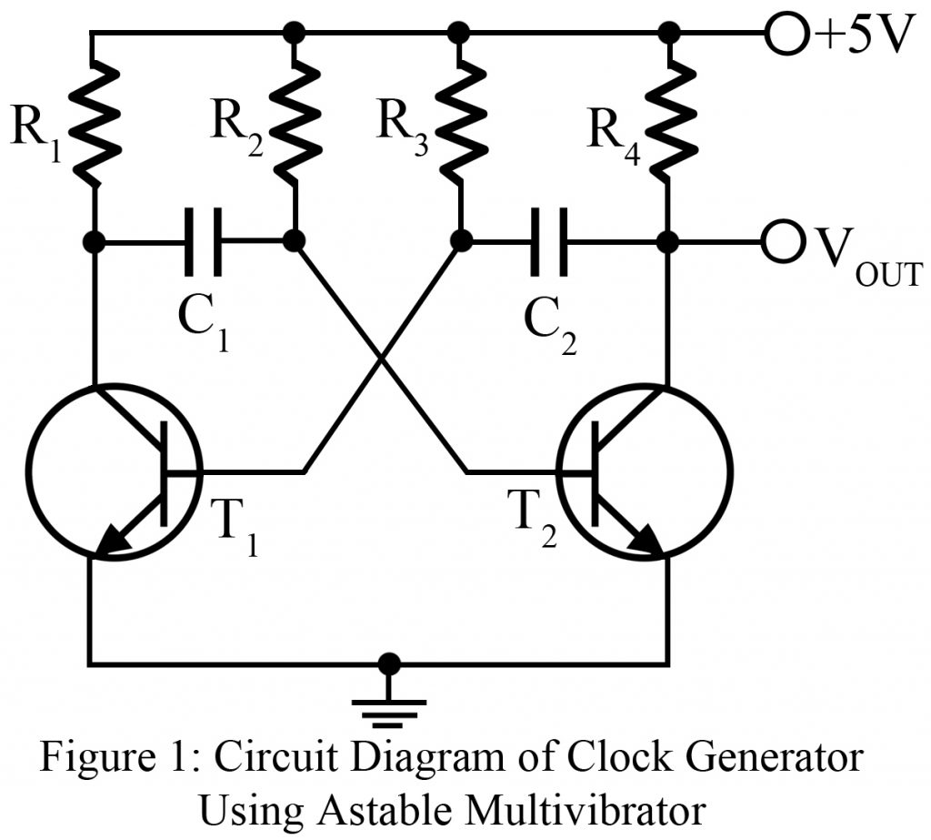
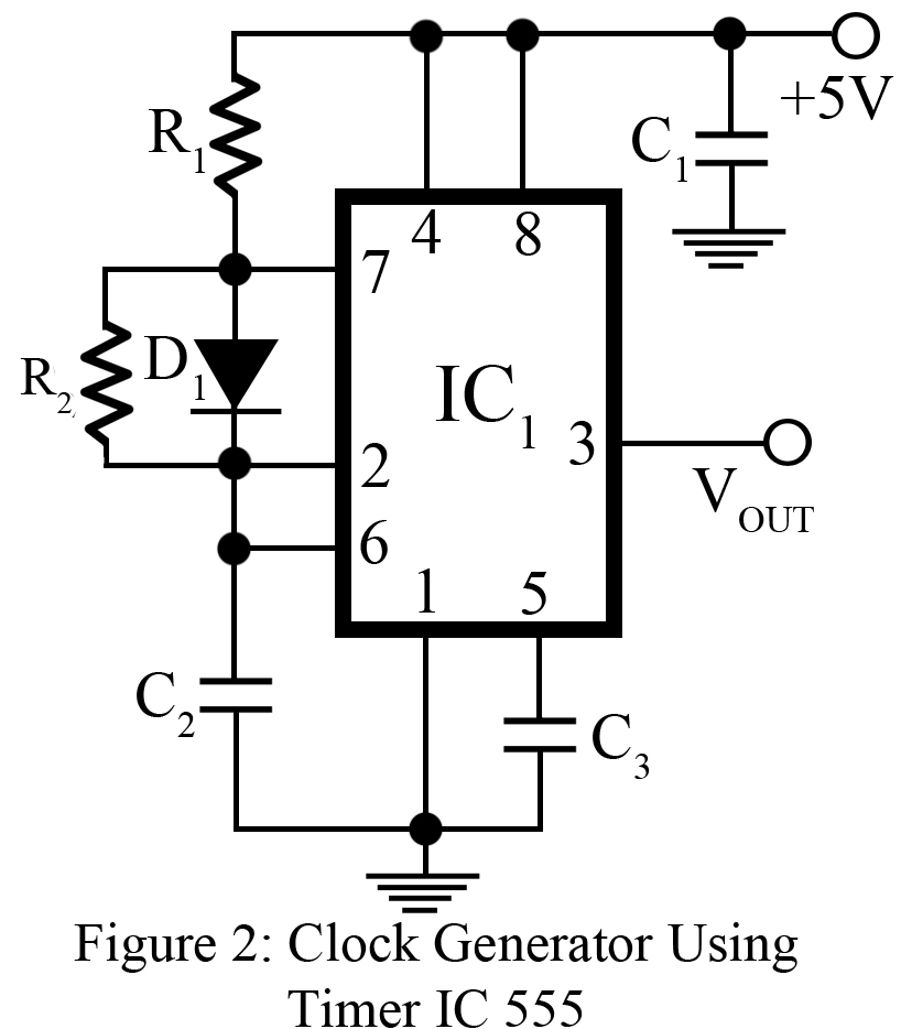
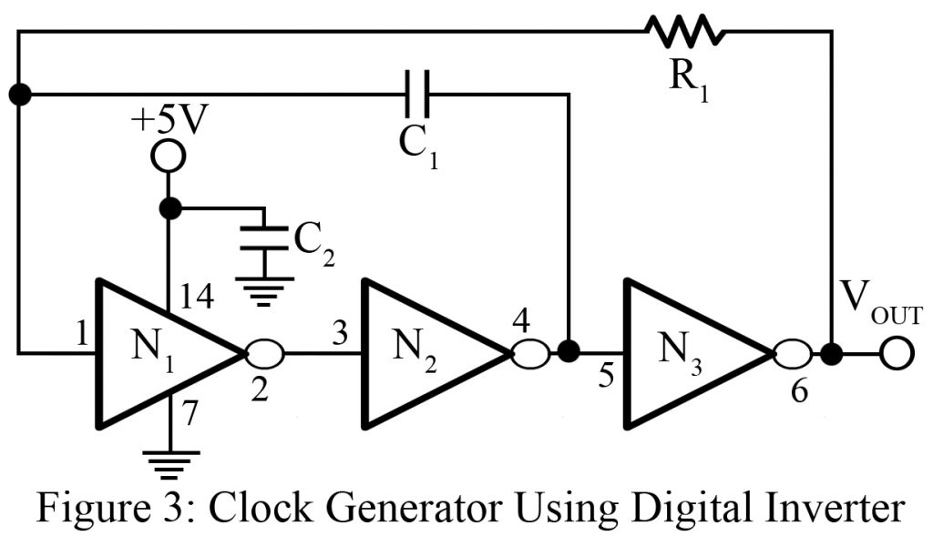
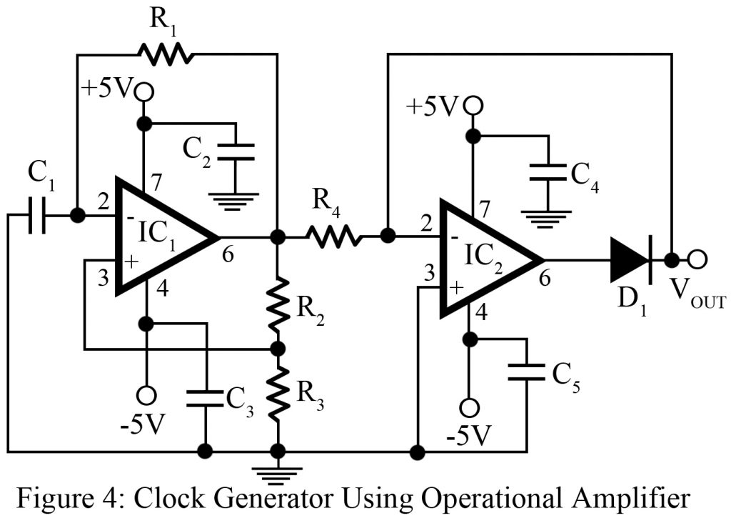
Circuit diagram of Clock Generators using Astable Multivibrator, Clock Generator using Timer IC 555, Clock Generator Using Digital Inverter IC, Clock Generator using OP-AMP
Objectives of Clock Signal Generator
You might have noticed a common thing in most digital integrated circuits, which is a frequent need for a continuous pulse train defined as a clock pulse for the precise operation of the circuit. Since most sequential logic devices such as flip-flops, counters, registers, etc. favor a synchronous mode of operation, the need for the clock is felt more pronounced in ICs that constitute those devices. To serve our needs, specialized clock generator ICs are distributed throughout the market.
However, these clock signals can be produced via many basic circuits. Doing that requires very basic components. Then, why shall we not invest a little time and effort to learn something new if it is worthy of our investments? I don’t see any reason not to do so when things can be managed so well without losing anything. Here we will develop four completely different clock generators each of which implements different devices: discrete devices, linear integrated circuits, and digital integrated devices.
It comes with a limiting factor; the clock pulse generated may not be as precise as generated by the designated circuit but this project is worth a try. Our sole aim is to generate a 1MHz clock signal from each of the four circuits and then evaluate the signal quality produced through each of them.
CIRCUIT DESCRIPTION OF CLOCK SIGNAL GENERATOR
We are discussing multiple ways of pulse generation and so it is obvious that this project constitutes several circuits. There are altogether four dedicated pulse generating circuits and one extra circuit to provide supply (DC voltage) to operate each of those circuits. A detailed description of each is given below:
-
Clock Generators using Astable Multivibrator
This is the first circuit for clock pulse generation as shown in fig 1 which employs basic and discrete components as an astable multivibrator and two bipolar transistors which are serially connected back to back. This makes it easy to extract output from any one of the collector pins of two transistors. As shown in the figure, if we use Q2 collector output, the time constant of combination R2 and C1 (=0.69R2C1) decides the high time of the output waveform. And in the same way, R3 and C2 time constant (=0.69R3C2) decides the low time of the waveform. The reverse occurs if the output is taken from the Q1-collector terminal. Due to this fact, we can say two different outputs obtained from Q1 and Q2 are inverted versions of each other.
Here let’s assume
R2 = R3 = R and C1 = C2 = C.
The expression for output signal frequency is given by
F=1/(1.38RC).
If we follow the table attached below for component values, 1 MHz is the approximate frequency value for this project.
One must be careful enough to use high-speed bipolar switching transistors (i.e. 2N918). If you are out for other switching transistors such as 2N 2222, one might notice deterioration in the waveform obtained along with rising and abrupt falling edges. The waveform may appear triangular rather than the pulsed one we expect as output. However, up to a few tens of kHz, this transistor works fine and may fit as the exact match.
PARTS LIST OF CLOCK GENERATOR USING ASTABLE MULTIVIBRATOR
| Resistor (all ¼-watt, ± 5% Carbon) |
| R1, R4 = 270 Ω
R2, R3 = 8.2 KΩ |
| Capacitors |
| C1, C2 = 100 pF (Ceramic Disc) |
| Semiconductors |
| T1, T2 = 2N918 (NPN Silicon RF Transistor) |
-
Clock Generator using Timer IC 555
The core component for this project is the most commonly used timer IC555. This circuit is fairly popular for the use of usually available components. The R1 and C2 time constant (0.69R1C2) supplies a high-time output waveform at pin no. 3 of IC. Similarly, low time output is provided by the time constant (0.69R2C2). If values from the table are picked, then these values of high and low time are calculated to be approximately 500 nanoseconds.
Thus, the frequency of the output waveform is nearly 1 MHz. The fact that all precise arrangements are made to extract a 1 MHz clock signal is obvious. However, the results obtained, mostly a wave shape lie far away from the satisfactory region. It is probably because the rising and falling edge of the waveform is far from being vertical. As a result of the consequences caused by the limiting factor of the internal circuitry of 555 timer IC, the waveforms tend to have triangular shapes instead of smooth square-shaped waveforms.
If you observe, you might have noticed we have used all the component’s values in such a way that they together generate an output of 1 MHz. The reason behind doing so is just because the timer IC cannot be used at that frequency. However, if you want, you can vary the values of components and check out the waveforms obtained at different output frequencies. You can evaluate the difference for yourself. The maximum limit for obtaining a fair clock signal wave shape is up to 100 kHz. Beyond that, the wave shape obtained may not meet our expectations.
PARTS LIST OF CLOCK GENERATOR USING TIMER IC555
| Resistor (all ¼-watt, ± 5% Carbon) |
| R1, R2 = 680 Ω |
| Capacitors |
| C1 = 0.1 µF (Ceramic Disc)
C2 = 0.001 µF (Ceramic Disc) C3 = 0.01 µF (Ceramic Disc) |
| Semiconductors |
| IC1 = NE555 (Timer IC)
D1 = 1N914 (Small Signal Fast Switching Diode) |
-
Clock Generator Using Digital Inverter IC
Had you looked through clock generator circuits before, you must have noticed a variety of circuits built cascading three inverters and an R-C circuit. A digital inverter clock generator is a similar circuit that encompasses CMOS hex inverter IC 4069. Another appealing fact about this circuit is that an R1 and C2 time constant given by 0.5R1C2 alone decides both the HIGH and LOW times of the circuit. The entire process revolves around the charging and discharging of the capacitor.
During the high output, the capacitor charges through R1, and for the low output, it discharges through the same resistor R1. As in the previous circuit, the output frequency is 1 MHz for the values of the components listed in the table.
PARTS LIST OF CLOCK GENERATOR USING DIGITAL INVERTER IC
| Resistor (all ¼-watt, ± 5% Carbon) |
| R1 = 1 KΩ |
| Capacitors |
| C1 = 1000Pf (Ceramic Disc)
C2 = 0.1 µF (Ceramic Disc) |
| Semiconductors |
| IC1 (N1 – N3) = 4069 (CMOS hex inverter) |
-
Clock Generator using OP-AMP
For the simplicity of understanding the working of the circuit, the circuit is divided into two distinct parts. IC-3 along with resistors R1, R2, R3, and capacitor C1 form up the first section which is a square wave oscillator. The peak amplitude of the positive and negative half cycle is approximately 5 volts. The oscillator output waveform is symmetrical with a period defined by
T = 2*R1*C1*Ln[(1+K)/(1-K)]
Where K = R3/(R2+R3).
As per the component values from the table, the expression
Ln[(1+K)/(1-K)] = 1
And the operating frequency equals 1/2*R1*C2=1 MHz.
Now moving on to the next section, the circuit is fabricated around IC-4, resistor R4, and diode D1. This combination of circuits is also called a half-wave rectifier since it only permits positive half cycles. The reasonable process behind this is described in detail in upcoming lines. For the square waveform input, during the positive half cycle, diode D1 is reverse biased and so it passes the positive part only, which is seen at the output part.
On the contrary, for the negative half, the diode becomes forward biased and the circuit crumbles into an inverting amplifier pattern that has a zero feedback resistance. Thus, the result obtained at the output is also zero. One must be aware enough to employ an AD829 op-amp and diode D1 (N914), both of which are high-speed devices. The precision of the value used is an important factor to generate a 1 MHz frequency.
PARTS LIST OF CLOCK GENERATOR USING OP-AMP
| Resistors (all ¼-watt, ± 5% Carbon) |
| R1 = 500 Ω
R2 = 10 KΩ R3 = 8.6 KΩ R4 = 1 KΩ |
| Capacitors |
| C1 = 1000 pF ((Ceramic Disc))
C2 – C5 = 0.1 µF (Ceramic Disc) |
| Semiconductors |
| IC1, IC2 = AD829 (low noise high speed op-amp)
D1 =1N914 |
CONSTRUCTION GUIDELINES
Figures 1, 2, 3, and 4 represent the four different choices. The project is so simple that it can be constructed easily on a general-purpose PCB. For testing, if observed values are correct, then one of the four output waveforms is selected at a time and then analyzed using an oscilloscope. Thus measured values are compared with theoretical values. Again, one must check on the result and observe the effects of analyzing.
Check out other top popular Articles :
Clock Signal Generator Circuit


