Many Inverter Circuits have already been posted on many other websites. The inverter circuit “Crystal Controlled Inverter” presented here provides a stable output frequency even when there is a change in the DC voltage applied to the inverter. This stable output of the Crystal control Inverter is obtained from the 3.2786 MHZ crystal (XTAL1). You can also make your 3000W inverter using a microcontroller.
Circuit Description of Crystal Controlled Inverter.
The Inverter circuit “Crystal Controlled Inverter” is built around popular flip flop IC MM 5369 (IC1) followed by a few other active and passive components. IC1 (MM 5369) contains 16 cascade flip flops, which divides the input frequency of 3.2786 MHZ by a factor of 216. Thus we get an output frequency i.e. 3,276,800 Hz/216=50 Hz.
The frequency of 50 Hz is available in pin 1 i.e. at the output of IC1 (MM 5369). The timer capacitor is used to adjust the resonant frequency of the crystal. The CMOS chip (MM 5369) cannot deliver or sink more than 10 mA, therefore a current amplifier is necessary to drive the driver or pre-driver stage of the Crystal Control Inverter.
The fundamental mode of crystal is 3.2768 MHZ and operates in this mode. The small change in the frequency of oscillation of crystal in Crystal Controlled Inverter is caused by trimmer C2. The trimmer C2 is also used to adjustment of damping in the network. C1 is also used to balance the network as trimmer C2 does. Resistors R1 is used as load and R2 is used to limit the current flowing through the chip. In the event of a reversal of polarity at the battery terminal, diode D1 serves as a protector of the IC1 (MM 5396).
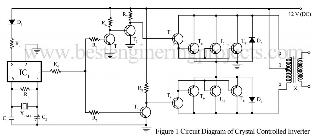
Resistors R3, R4, and R5 are used as a current splitter to share the current in the base of the transistor drive from the chip. For total inversion of 3600 and 00 transistors T1 and T2 are used as an inverter. Transistor T3 is also connected as an inverter and the output at the collector of T3 is at a phase difference of 1800 concerning the signal at the collector of transistor T2. Transistors T4 & T6, T7 & T8, and T5 & T9, T10 & T11 are connected as Darlington pair configuration as shown in the circuit diagram of Crystal Controlled Inverter.
The advantage of this type of configuration in Inverter Circuits is, that it provides enough base drive for the power stage to flow through the transformer which is connected to T4 and T5. This also increases the efficiency of the Inverter, because, in this configuration, additional current flows through the transformer rather than through the resistor and is dissipated as heat in them. The excessive PIV generated in the transformer due to the switching action of the power transistor is protected by diodes D2 and D3. The transformer used in Crystal Controlled Inverter is of step-up type 270VAA with a primary of 9V-0V-9V/15A and a secondary of 230V. You can also use 230V, 9-0-9V/15A, and 270VA step-down transformer which is used in the circuit exactly the other way round and works and works satisfactorily.
Check out other power supply and inverter circuit posted on besengineeringprojeccts.com
- Offline UPS Circuit
- Advance Emergency Light Circuit
- 3000W Inverter with Inbuilt Charger using AT89C2051
- Advance Mini UPS
BEP LAB NOTE
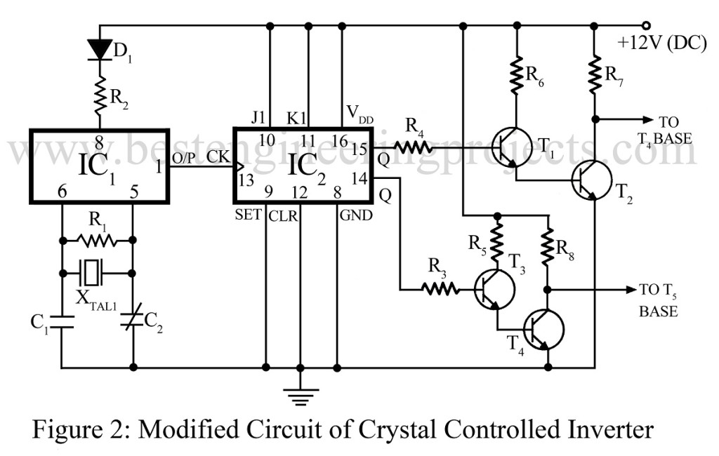
It is observed in BEP LAB that the division factor of IC1 (MM 5369) is not 216=65,536 but 60,000 and its frequency using an XTAL1 of 3.2768 MHz equals 54.6Hz. To obtain an exact frequency of 50Hz in outputs of Crystal Controlled Inverter, one may use an XTAL1 of 6 MHz to obtain 100 Hz and follow it up with a flip-flop to obtain a symmetrical (square wave) 50 Hz output. The modification circuit of the Crystal Control Inverter is given here.
PARTS LIST OF CRYSTAL CONTROLLED INVERTER
|
Resistor (all ¼-watt, ± 5% Carbon) |
|
R1 = 22 MΩ R2 = 100 Ω R3, R4, R5 = 1 KΩ R6, R7 = 120 Ω R8 = 129 Ω/1W |
|
Capacitors |
|
C1 = 33 PF (Ceramic Disc) C2 = 22 PF (trimmer) |
|
Semiconductors |
|
IC1 = MM5369 (17 Stage Oscillator Divider) D1 – D3 = 1N4001 (Rectifier Diode) T1 – T3 = C1384 (NPN Transistor) T4 – T11 = 2N3055 (Mounted in heat sink) |
|
Miscellaneous |
|
XTAL1 = 3.2768 MHz X1 = 230V AC primary to 9V-0V-9V, 15A secondary (270VA) step down transformer Heat Sink |
PARTS LIST OF MODIFIED CIRCUIT OF CRYSTAL CONTROLLED INVERTER
|
Resistor (all ¼-watt, ± 5% Carbon) |
|
R1 = 22 MΩ R2 = 100 Ω R3, R4 = 2.2 KΩ R5, R6 = 470 Ω R7, R8 = 120 Ω |
|
Capacitors |
|
C1 = 33 PF (Ceramic Disc) C2 = 22 PF (trimmer) |
|
Semiconductors |
|
IC1 = MM5369 (17 Stage Oscillator Divider) IC2 = CD4027 (Dual JK Flip Flip) D1 = 1N4001 (Rectifier Diode) T1, T3 = BC147 (NPN Silicon Transistor) T2, T4 = SL100 (Medium power, Silicon NPN Transistor) |
|
Miscellaneous |
|
XTAL1 = 6 MHz |
Good day admin…can u upload inverter circuit using 4047 with full battery monitoring.