Wireless Mobile Charging is one of the trending topics in the field of electronics thus we also decided to build a Wireless Mobile Charger Circuit Diagram using various commonly available components. The project Wireless Mobile Charger Circuit Diagram posted here can deliver 271mA at 5.2V so you charge mobile phones and also can be used to drive low power loads such as LED1 and LED2 as shown in figure 2.
Working Principle of Wireless Mobile Charger Circuit Diagram
Wireless Mobile Charger uses the inductive coupling principle. In this principle, two LC-tuned circuits communicate at the same tuned frequency i.e. tuned frequency of the transmitter must be equal to the tuned frequency of the receiver. Here, we had to use LC-tuned to produce and transfer the magnetic field which is received by another LC-tuned circuit.
Circuit Description of Wireless Mobile Charger Circuit Diagram
For simplicity and better description, we have divided Wireless Mobile Charger Circuit Diagram into sections i.e. transmitter circuit and receiver section
Transmitter Circuit for Wireless Mobile Charger Circuit Diagram: –
The transmitter circuit of the Wireless Mobile Charger Circuit Diagram is shown in figure 1 and is built around timer IC 555, a general-purpose NPN transistor BC547, N-channel MOSFET IRF540N, LC-tuned circuit, and a 5-volt series voltage regulator 7805.
![]()
Let us first talk about what a tuned circuit is? In the above circuit, we used a tuned collector oscillator (L1 with C1 and C2). The tuned collector oscillator uses a parallel L-C circuit in the collector circuit as the load and this circuit determines the frequency of oscillation. The output voltage developed across the tuned circuit is inductively coupled to the base circuit.
Timer IC 555 is used here for pulse generation thus it is arranged in astable multivibrator mode. The output of IC 555 (pin 3) is connected to the base of the general-purpose transistor T1 which is used to drive the MOSFET T2. The MOSFET T2 is used to switch the L-C tuned circuit which further transmits the oscillating magnetic field.
Series voltage regulator IC2 is used to provide operating voltage for the entire circuit (+5V) from +12V as shown in figure 1.
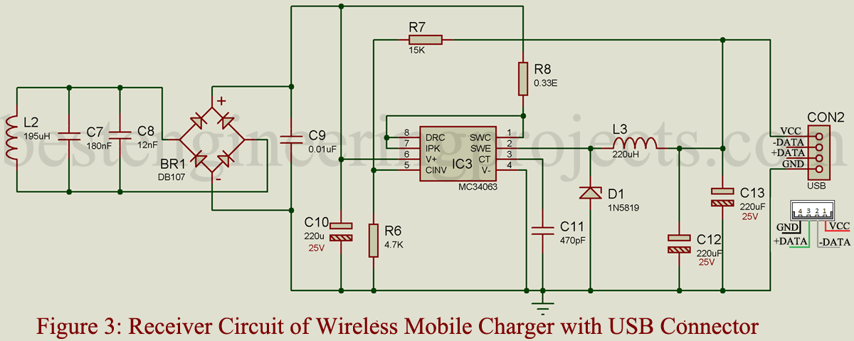
Receiver Circuit for Wireless Mobile Charger Circuit Diagram: – Receiver circuit shown in figure 2 is built around LC tuned circuit (L2 with C7 and C8), a current regulator (buck and boost) IC MC34063, Schottky diode (1N5819), and a few passive components. The transmitted oscillation magnetic field is detected by L-C tuned build around inductor L2 with capacitors C7 and C8 which is further changed to DC voltage using bridge rectifier BR1 and filtered using capacitors C9 and C10.
![]()
The ripple-free DC voltage is now given to buck/boost IC, configured into buck regulator mode. The output voltage is further filtered using an L-C filter and is connected to LED through current limiting resistors R9 and R10.
Receiver Circuit for Wireless Mobile Charger with Female USB Connector: The receiver circuit for the mobile charger shown in figure 3 is a little different than the receiver circuit posted above in figure 2. Both the LED (LED1 and LED2) is replaced by a female USB connector. Connect the female USB as shown in figure 3. VCC (RED wire) is connected to the positive terminal of capacitor C13 where GND (Black wire) is connected to the circuit ground. Both the data pin (D- and D+) is not connected.
PCB Construction for Wireless Mobile Charger Circuit Diagram: – The actual size solder side PCB design and component side PCB design of the transmitter circuit of the Wireless Mobile Charger Circuit Diagram are shown in figure 3 and figure 4 respectively. Similarly, figure 5 and figure 6 show the solder side and component side of the receiver circuit of the Wireless Mobile Charger Circuit Diagram.
![]()
Figure 4: Solder Side PCB of Wireless Mobile Charger Circuit Diagram Transmitter
![]()
Figure 5: Component Side PCB of Mobile Charger Circuit Diagram Transmitter
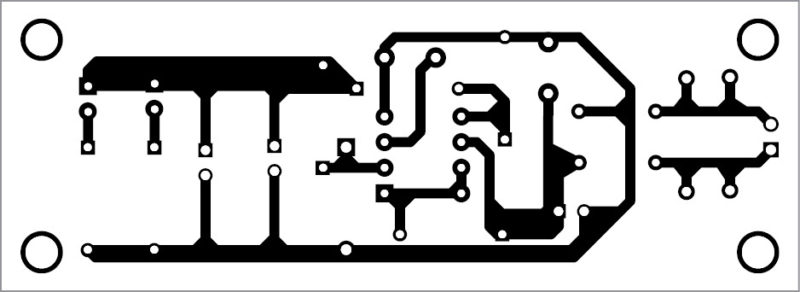
Figure 6: Solder Side PCB of Mobile Charger Circuit Diagram Receiver
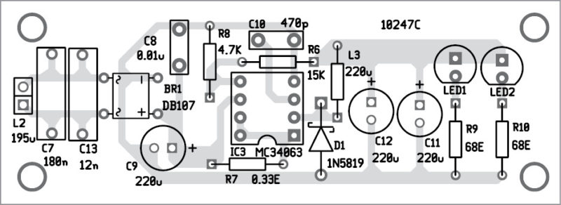
Figure 7: Component Side PCB of Mobile Charger Circuit Diagram Receiver
Click Here To Download the PCB Diagram
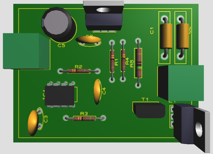
Figure 8: 3D View of Wireless Mobile Charge Transmitter Circuit

Figure 9: 3D View of Wireless Mobile Charge Receiver Circuit
Math’s involves in Wireless Mobile Charger Circuit Diagram
The entire calculation shown below is done by considering the parts list value in this circuit.
- Transmitter Circuit: – As the 555 is wired in an astable multivibrator thus we have to calculate pulse oscillation.
Charging time = 
Discharging time = 
Oscillating Frequency of 555 = 
LC Tuned Frequency 
Where L = L1 = 180µH
C = C1 + C2 = 0.1µF + 0.1µF = 0.2µF
Therefore, 
- Receiver Circuit: –
LC-tuned frequency must be equal to the transmitter-tuned frequency of 26 kHz. Thus,
Where, L = L1 = 195 µH
C = C7 + C8 = 180nF + 12nF = 192 nF

- Output Voltage


Vref of IC3 = 1.25V
R7 = 15 KΩ
R6 = 4.7 KΩ
Therefore, Output Voltage (VO) = 5.2V
Output Current = 271mA
Power Output = 
Input Voltage = 12V
Input Current = 180mA
Power Input 
Now, we can calculate 
Note: You can increase the efficiency of the circuit by using a magnetic core instead of an Air Gap as shown in Figure 7.
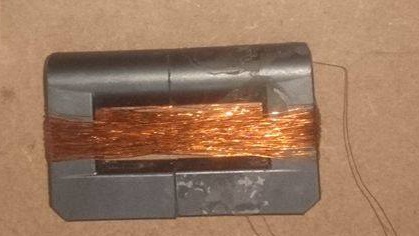
Figure 8: Magnetic-Code Inductor Coil
PARTS LIST OF WIRELESS MOBILE CHARGER CIRCUIT DIAGRAM
| Resistor (all ¼-watt, ± 5% Carbon) |
| R1, R4 = 1 KΩ
R2, R3 = 3.3 KΩ R5 = 150 Ω R6 = 4.7 KΩ R7 = 15 KΩ R8 = 0.33 Ω R9, R10 = 68 Ω |
| Capacitors |
| C1, C2 = 0.1 µF (Polyester Capacitor)
C6 = 0.1 µF (Ceramic Disc) C3, C4, C9 = 0.01 µF (Ceramic Disc) C5 = 100 µF/25V (Electrolytic Capacitor) C7 = 180 nF (Polyester Capacitor) C8 = 12 nF (Polyester Capacitor) C10, C12, C13 = 220 µF/25V (Electrolytic Capacitor) C11 = 470 pF (Ceramic Disc) |
| Semiconductors |
| IC1 = NE555 (Timer IC)
IC2 = LM7805 (Series Voltage Regulator, 5V) IC3 = MC34063 (Buck/ Boost Regulator IC) D1 = 1N5819 (Schottky Diode) T1 = BC547 (General Purpose NPN Transistor) T2 = IRF540N (N-Channel MOSFET) BR1 = DB107 (Bridge Rectifier) LED1, LED2 = 1-watt LED |
| Miscellaneous |
| L1 = 180µH inductor using a 35-turn, 50mm diameter of 26SWG enameled copper wire
L2 = 195µH inductor using a 45-turn, 50mm diameter of 26SWG enameled copper wire L3 = 220µH Fixed Inductor CON1 = 2-pin Terminal Connector Heat Sink for Series Voltage Regulator (7805) CON2 = Female USB Connector |
Thankyou very much sir.
i was searching for this projects since long.
is this projects works.
01
has any one done this project for real,as i will be doing this for my collage and so would you like to give me any advice related this project??please reply asap.
The project wireless mobile charger posted here is 100% verified.
Here in the link below we had posted the author prototype
https://www.facebook.com/BestEngineeringProjects/posts/1528539337195340
THANK YOU VERY MUCH
you made things really clear and simple for me?
your efforts are very much appreciated
sir in the output circuit from where do we take output to the cell phone
For output you have to replace both the LEDs (LED1 and LED2) with USB connector where positive terminal is connected to positive leads of capacitor C13 and negative terminal is connected to negative terminal of capacitor C13.
please help asap
Thanky sir just one last thing is it possible to convert 220 volt ac to a 12 v 180mA for input in transmitter circuit
sir how to convert 220v ac to 12 volt 180mA dc in order to supply the transmittor
Sir con i use 12v 1 amp adaptor as source in the transmitter circuit
*can
Pleade reply asap please
My project is stuck with the source part rest of it is sorted please help
What source part can you please elaborate please?
in the transmitter side you can use 12V 1 amp. adapter or you can make your own 12V power simple 12V power supply.
Sir in the transmitter circuit can we use 12 volt 1 amp adapter as in the calculations you are saying 12 v 180 ma
The circuit designed here draws 180mA at 12V this doesnot not mean you have to use 12V supply at 180mA.
Any supply which gives more then 180mA at 12V output can be used here, because any system draw current as per requirement not as per supply. So you can use use adapter of 12V at 1amp.
if you have any further queries then please summerize all in one comment thankyou.
Thank you for your quick response.
Can i call or watsapp you please
Please help sir it is urgent
Thank you so much
You guys are the best
can i use this circuit to charge any phone or specific type of phones. And if i want to charge phone battery to charge an electrical car. is that can be possible ??
thank you so much sir
this circuit works well
thank you for your constant support
https://uploads.disquscdn.com/images/31ec008fa7ecb1fb8f2b9208d4c2ff265b697ef173eb137004c3d7d530ba5c37.jpg
What is the range of the charger…
Depends upon the coil you have used.
well documented !! …one question please
what software did you use for PCB designing ???
thanks for help….
We had used various type of software like Proteous, Altium ect.
Hello, if i want to use to charge the smartphone. How to increase the receiver side output to 5V 1.5A. Thank you very much
sir what is the range of induction?if we use 37swg instead of 26 swg.shouldthe no.of turns be higher to match the induction.
Sir,what is the range (distance) of induction? If we use 37swg instead of 26swg should the no of turns be higher to match the inductance
sir how many turns are required if we change the swg to 37 from 26
how to calculate it sir?
High swg wire means larger cross section area. Thus, used for high current.
So i suggest you to use 37 SWG of wire.
Sir when I give 12 volts power supply to the transmitter circuit the 180uH inductor is getting heated up and there is no power transmission from the transmitter to the receiver circuit.Can u help me in rectify this problem?
please make sure about current rating of your coil.
Generally coil heat-up due to resistive loss.
my mosfet part is not activated. do you know what might be the reason?
At first please check the entire connection, if every this is fine then check whether transistor become on or not by using multimeter. If every thing is fine then your mosfet might have issue replace it.
what is value of mutual inductance between the coils sir.
Hai sir…Can I replace the L3 with some other resistor. That inductor is not available to us…plzz reply I have taken your project for my college mini project…..plz reply
Hello,
Sorry, you cannot replace inductor with resistor.
Okk thanks sir for your quick response
Sir, can i replace L3 220uh fixed inductor with 330uh or 100 uh fixed inductor..please response first sir…
I have not tested it yet, but you can give it a try.
But, I would recommend you to join two 100uh inductors in series.
Okk thanks sir..sir that inductor is used for filtering purpose so can i use 150uh…And sir i have tested the transmitter side by giving 12v… but the mosfet is getting very hot. What is the problem. I have checked the circuit and it is very perfect
Please recheck the circuit connection, heating of MOSFET is mainly due to the flow of large current when the gate is not fully opened.
I was selected this as my project and a have completed transmitter side circuit so how can i check that my circuit is working well or not or what is the output voltage at coil terminal by which i can understand my circuit is working
please help me
It’s better to check the output frequency of the transmitter circuit rather than voltage.
hello sir,
as i am doing this project i was completed the transmiter and receiver part of wireless charger circuit but i stuck in a problem that my transmitter part is not working as i am not able to measure the output frequency so i measure the voltage but at 1st and 3rd terminal from vcc of IRF540 mosfet shows approximately 12v but at the 2nd terminal (o/p) zero volage shows and it not work properly
so please help mi sir this is very urgent
hellow sir now my project is working
but 1 thing i want to ask that what very small noise are coming from my transmitter and can i stop this noise
Glad to know that project is working
There might be two reasons for noise
1. There might be piezoelectric effects in ceramic capacitors. This is due to a change in voltage across capacitors (C1 and C2).
2. Another reason is magnetostriction in an inductor L1.
Do you use core in inductor L1?
Because core materials produce humming sound when the magnetic flux density changes.
Please Sir, any video for this project, to serve as a guide. Thanks a lot
Hello sir, this project worked just fine as I used it for my final school project.
I want to build another with a higher current output, is it the number of turns of coil I need to increase? What other thing should be increased?
Sir, We’re doing this as our project for university. We connected everything as indicated here. But the Transmitter circuit output voltage is very small normally but when the heat sink of mosfet i touched it shows a 7V output. What might be the problem and what can we do to fix it? Hoping for a reply asap. Thank you!
Sir, We’re doing this as our project for university. We connected everything as indicated here. But the Transmitter circuit output voltage is very small normally but when the heat sink of mosfet i touched it shows a 7V output. What might be the problem and what can we do to fix it? Hoping for a reply asap. Thank you!
is there any way we can the schematics so we can download them and run it
Hello, good time, I had a question about the coils, how many turns should the coils be wound and what is their diameter??
I mean the number of twists
Hello Sir,
Did you make the card designs using the PCB diagrams available on your website?
When I did the circuit printing, some of the components did not match the holes.
Can you help me?
Thank you so much in advance.
But the transmitter circuits diagram is different with the pcb designed!
Please which one to follow?
Hello
Can this transmitter circuit deliver 7 W – 10 W to charge a mobile phone?
If so ? how many windings does my coil has to have? Or how can I calculate that?
Dear sir
Is it possible to give output 12-24v for it will be amazing if I can recharge my e-bike batteries wirelessly? Please enlight me