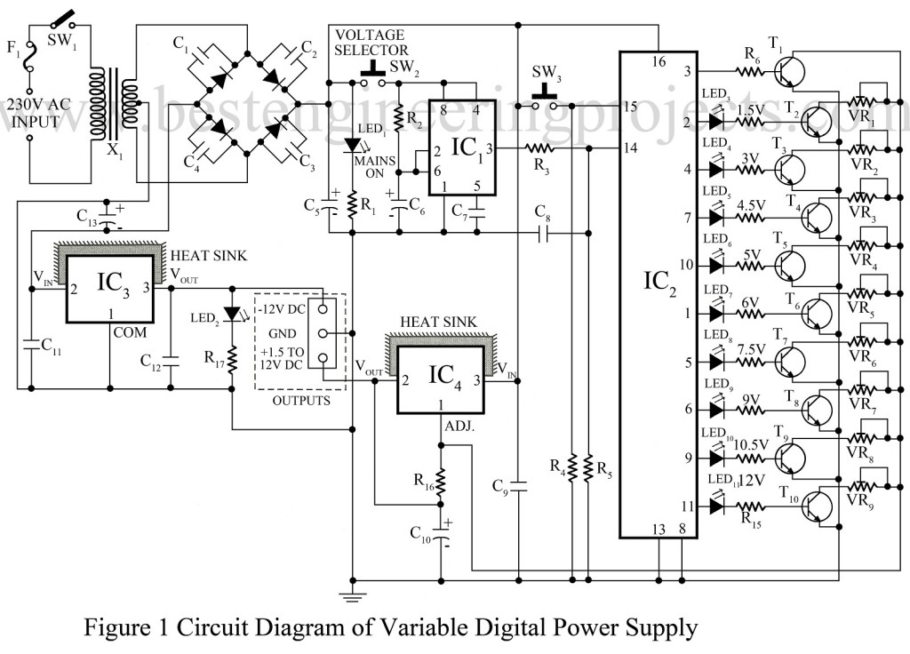
Various types of power supply circuits like fixed regulated, variable power supply, and stabilized power supply circuits are already published on bestengineeringproject.com. Most of us hear about the universal power supply, it is a power supply unit that provides almost all standard power supply. How’s that if we combine a universal power supply and a digital control technology. Here, the innovative group of Dreamlover Technology designed and verified a universal power supply circuit with the facility of digital control. The unit universal digital power supply provides a variable, fluctuation-free and regulated output.
Circuit description of the universal digital power supply circuit
The circuit of the universal digital power supply comprises an adjustable 3-terminal positive voltage regulator IC (Lm317), decode counter IC (CD4017), timer IC (NE555), and a fixed-negative-voltage regulator (Lm7912). The input AC of 220V is steeped down by using transformer 12V-0-12V, 1A secondary. The step-down voltage is rectified using a bridge rectifier built using diode D1 through D4 parallel-connected capacitor C1 through C4 is for bypassing undesired spikes and providing smooth and function-free power.
For extra filter and to eliminate ripple capacitors C5 and C13 are used. Here both positive and negative power supply is utilized and fluctuation-free output is obtained. Timer IC NESS (IC1) is wired as an astable multivibrator and generates clock pulse when switch SW2 is pressed switch SW2 is also used as voltage selector. The output of IC1 from pin 3 is given to clock pin 14 of IC2 through the RC network built by resistor R3 and capacitor C8. IC2 is a decade ring counter IC and utilizes all the outputs switch SW3 is connected to reset pin 15 and is pressed to reset IC2.
The output of IC2 is connected to the base of transistor T1 through T10 through resistor R6 through R11 respectively preset VR1 through VR9 is connected to the collector of transistor T2 through T10 respectively for voltage adjustment LED3 to LED11 is used to indicate 1.5V, 3V, 4.5V, 5V, 6V, 7.5V, 9V, 10.5V, 12V DC respectively. Negative 12 volts (-12v) DC is obtained at the output of IC3 and is indicated by LED2. IC3 is a fixed 3-terminal negative voltage regulator and produces regulated -12V DC.
IC4 is an adjustable voltage regulator and its output voltage obtained is dependent upon the reference voltage between its output and the adjustable terminal. IC4 develops a 1.25V normal reference voltage and appears across R16. The output at pin 4 of IC4 is calculated by using the formula Vout=1.25(1+VRset/R16).
Where VRset is preset VR1 through VR9. Adjust preset VR1 through VR9 to get desired output. The collector of transistor T 5 is directly connected to the ADJ terminal (pin 1) of IC4, so the output voltage of IC4 will be the voltage across fixed resistor R16 which is equal to 1.25V. By using a properly calibrated digital multi-meter you can easily adjust the presets to obtain 1.5V to 12V. Where IC2 is reset by using switch SW3 the output voltage at pin 4 of IC4 is 1.2V and all the voltage-indication LEDs are off.
Glowing LED1 is used to indicate mains ‘on’. Use proper heat sink for the voltage regulator IC (IC3 and IC4). Since pin configuration these ICS are different so never fix a single heat sink for both ICs.
Check out other power supply circuit posted on bestengineeringprojects.com
- Adjustable Ripple-Regulated Power Supply Using 741
- Variable Switching Power Supply
- Arduino Controlled Variable Power Supply
- Stabilized Power Supply With Short-Circuit Indication
- Short Proof Variable Power Supply
- Adjustable Bipolar Voltage Regulator Circuit Using LM337
- Self Switching-off Power Supply
- Dual Polarity 5v from 9v Battery
- 3.7V to 5V, 5.3V and 6V Converter Circuit
PARTS LIST OF UNIVERSAL DIGITAL POWER SUPPLY CIRCUIT
|
Resistor (all ¼-watt, ± 5% Carbon) |
|
R1, R7 – R15, R17 = 1 KΩ R2 = 22 KΩ R3 = 560 Ω R4, R5 = 8.2 KΩ R6 = 10 KΩ R16 = 220 Ω VR1 = 100 Ω VR2 – VR4 = 1 KΩ VR5 – VR7 = 2.2 KΩ VR8, VR9 = 4.7 KΩ |
|
Capacitors |
|
C1, C4 = 47 nF (Ceramic Capacitors) C5, C13 = 2200 µF/25V (Electrolytic Capacitors) C6 = 10 µF/25V (Electrolytic Capacitors) C7 = 0.01 µF (Ceramic Capacitors) C8, C9, C12 = 0.1 µF (Ceramic Capacitors) C10 = 1 µF/25V (Electrolytic Capacitors) C11 = 0.22 µF (Ceramic Capacitors) |
|
Semiconductors |
|
IC1 = NE555 (Timer IC) IC2 = CD4017 (Decade Counter IV) IC3 = LM7912 (Negative 12 Voltage regulator) IC4 = LM317 (Positive variable voltage regulator) T1 – T10 = BC548 (General purpose NPN Transistor) D1 – D4 = 1N4007 (Rectifier Diode) |
|
Miscellaneous |
|
LED1 = RED LED LED2 = YELLOW LED LED3 – LED11 = GREEN SW1 = ON/OFF Switch SW2, SW3 = Push-to-on Switch F1 = 1A Fuse X1 = 220V AC Primary to 12V – 0 – 12V, 1A Secondary transformer Heat Sink |

Thank you sir, i also want this type of circuit.