In this article, we will discuss about Sample and Hold Amplifier IC, its key parameters and its applications. But before that, let us see what a sample and hold circuit is. The principle underlying the digital signal processing is that of sampling the analog signal. Sampling basically means obtaining the discrete time signals from the reduction of the continuous time signals. The Nyquist–Shannon sampling theorem is one of the well-known and commonly used sampling theorem in signal processing. A sample and hold circuit obtains samples of an analog signal and hold them in the form of charge in capacitor. The voltage on the capacitor we obtain are the samples of the signal we are looking for. Each of these voltage levels is then fed to the input of Analog to Digital Converter, which provides an N-bit binary number proportional to the value of signal sample. Check this Three Bit Flash Analog to Digital Converter. The Sample and Hold Amplifier is extensively used in linear systems. Along with that, it works just like an operational amplifier i.e., we can design integrators, filters, and so on.
Description of Sample and Hold Amplifier IC
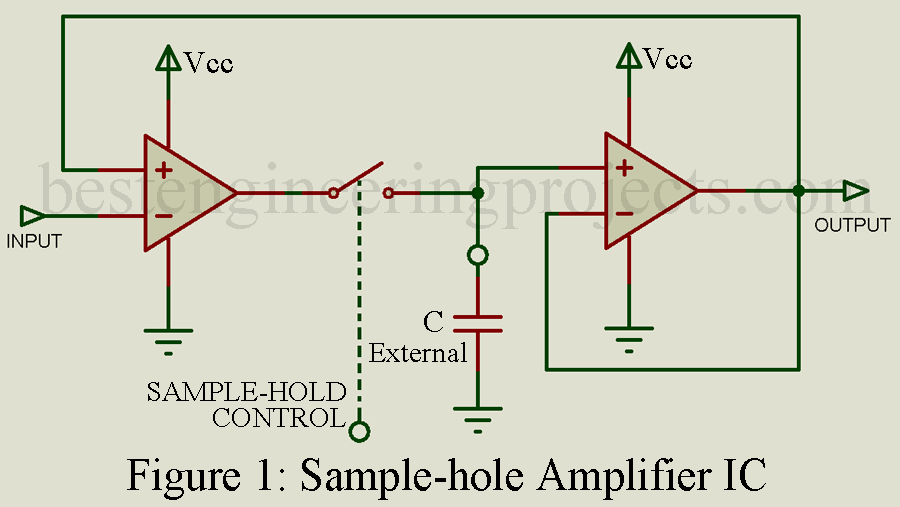
This amplifier IC generally consists of two op-amps with an electronic switch connected between them and a charging capacitor usually as an external component. As illustrated in figure 1, the amplifier operates in the sampling or tracking mode when the switch is closed. The output signal follows the input signal, usually with unity gain. When the switch is opened, the output signal remains at the previous value until the closing of the switch changes back to the sample mode. The sampling capacitor is usually connected either as shown in figure 1 or as the series feedback element of the op-amp closest to the output.
Key Parameters
- Acquisition time: The time required to reach the final output value after the “Sample” command. A value from 0.5 to 5.0
 is typical.
 - Aperture or delay time: The time required for the switch to open after the “hold” command. A typical value is from 150 to 500 ns.
- Aperture or delay jitter: The range of aperture time variation. 0.25 to 5 ns is typical.
- Charge transfer or offset step: The effect of stray capacitance during the “hold” mode. A value of 0.025% is typical.
- Droop: The loss in output voltage during the “hold” period, due to leakage current. Typical value are 50 pA to 10 nA leakage current.
- Feedthrough: The amount of AC signal coupled through the switch in the “hold” mode.
 is typical.
Applications
Sample-hold amplifiers are used in data acquisition and data distribution systems, in input stages of analog-to-digital converters, and for peak measurements of analog values.
Representative Part Number: Signetics NE/SE5537
Comments
Sample-hold amplifiers can be constructed of two op-amps and an analog switch, but the monolithic construction of the same amplifiers in a single IC provides the advantage of better temperature drift performance, and also requires much less space. Sample-hold ICs are available for high-speed applications.