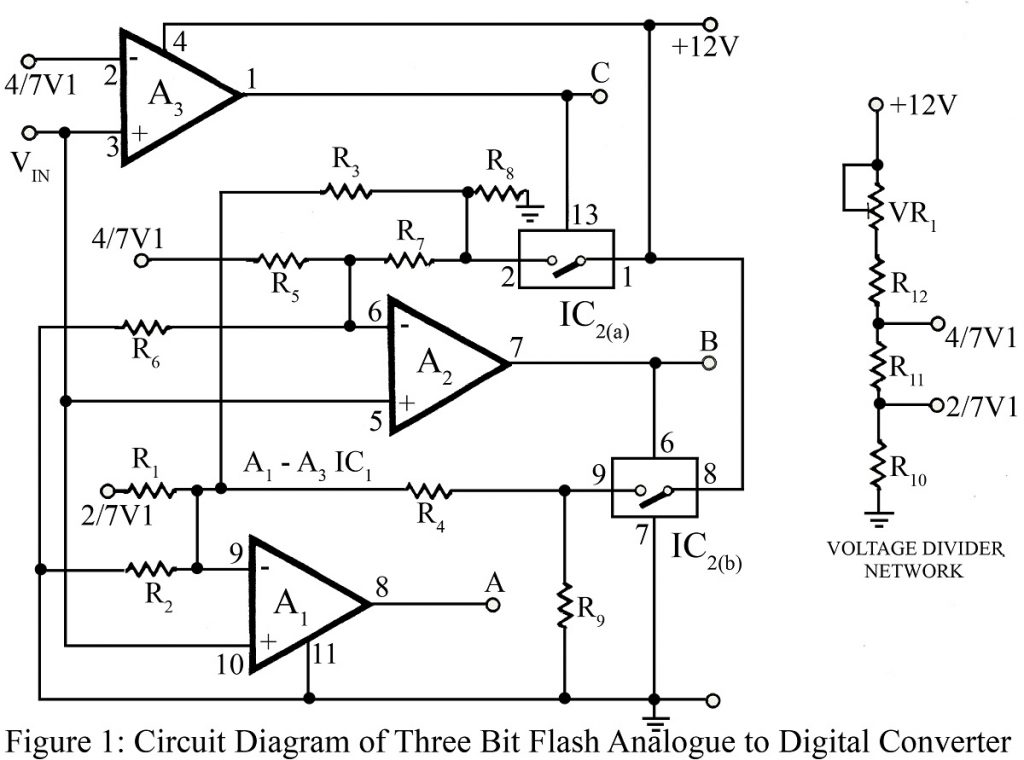
The flash type converter is the simplest and the fastest type of analog to digital converter. The entire digital output word is present just after the propagation delay time of comparators and the encoding logic gates. A typical conversion time of a three-bit flash analog to a digital converter is 33 ns. The circuit of a three-bit flash analog to digital converter shown in figure 1, needs just three comparators and no combinational logic circuitry.
Circuit Description of Three Bit Flash Analog to Digital Converter
In this circuit, the reference voltages on inverting inputs of the comparators are not fixed but dynamic. They change depending upon the state of the output of other comparators.
Non-inverting inputs of comparators A1, A2, and A3 are given an input voltage of 5 volts maximum. Inverting terminal of A1 is given VIN,/7, i.e. 0.714 volts where VIN is the full-scale voltage which is 5 volts in three-bit flash analog to digital converter. This is achieved by providing 2 VIN/7 to voltage divided formed by R1 with R2, R3, and R4 in parallel.
Similarly, inverting terminal of A2 gets 2 VIN/7, i.e. 1.42 volts which is achieved by dividing 4 VIN/7 into two parts by using a voltage divider comprising R5 with R6 and R7 in parallel.
To the third comparator 4 VIN/7, i.e. 2.857 volts is directly given.
When the input voltage is zero, outputs of all comparators are zero, giving binary 000. When input voltage crosses the VIN/7 level, the output of A1 becomes high, giving us binary 001. When an input goes slightly above 2 VIN/7, the output of comparator A2 becomes high which makes switch SW1 on, thus connecting the other end of R4 to +12V volts. This end was previously connected to the ground effectively.
Now voltage at inverting terminal of A1 rises to 3 VIN/7, i.e. 2.14 volts and the output of A1 becomes low, giving us output in direct binary 010. When an input goes above 3 VIN/7, the output of A1 also becomes high giving output 011.
A similar process is followed in higher input voltage, giving us an exact 3-bit binary. Values of all resistors are calculated by considering the increment in reference voltage concerning out-puts of other comparators.
Analog switches IC2 are used to provide exact 12 volts.
In this table outputs at expected and observed values are given, which clearly shows the accuracy of this crude circuit idea.
The voltage divider used in the circuit three-bit flash analog to a digital converter to get a fixed reference voltage.
| Step Voltage | Binary Output | Desired Voltage | Observed voltage | % Error | ||
| C | B | A | ||||
| 0VIN/7
2 VIN/7 3 VIN/7 4 VIN/7 5 VIN/7 6 VIN/7 7 VIN/7 |
00
0 0 1 1 1 1 |
00
1 1 0 0 1 1 |
01
0 1 0 1 0 1 |
00.714
1.42 2.14 2.857 3.75 4.28 5 |
00.732
1.46 2.09 2.9 3.47 4.24 4.9 |
-2.52
-2.8 2.33 -1.5 2.8 0.934 2.00 |
PARTS LIST OF THREE BIT FLASH ANALOG TO DIGITAL CONVERTER
|
Resistors (all ¼-watt, ± 5% Carbon) |
|
R1, R5 = 33 KΩ R2 = 115.6 KΩ R3 = 69.2 KΩ R4 = 138.6 KΩ R6 = 64 KΩ R7 = 68 KΩ R8, R9 = 1 KΩ R10, R11 = 100 Ω R12 = 560 Ω VR1 = 100 Ω |
|
Semiconductors |
|
IC1 (A1 – A3) = LM324 IC2 (IC2a – IC2b) = CD4066 |
You may also like:
- 4-Line to 16-Line Decoder Circuit using 7442 IC
- Pulse Generator cum Timer Circuit
- 1/86400 Hz frequency Generator Circuit

Where is the v1/7 and why do you used 4v1/7 two times in the circuit .
Can you tell me how exactly you are giving input .
In this circuit maximum input voltage is 5v as i mention above. Here V1/7 means input voltage is divided by 7 i.e. 5V/7 = 0.7142V and similarly 4V1/7 = 4*0.7142 = 2.85V.
Here we use a 4V1/7 directly to op-amp A1 and another v1/7 to op-amp A2 through resistor R6 in order to change it into 3V1/7V.
And finally input is given to the non-inverting terminals of op-amps
You say in theory R1 with R2, R3 and R4 in parallel. R5 with R6 and R7 in parallel.
but that are not in parallel .