Here in this article we are going to discuss about forward and reverse biased PN diode. We had also derive the equation and solve a numerical example. At first let’s see the reverse biased pn diode. Reverse Biased PN Diode Figure 1 shows a PN diode with reverse bias i.e. with negative terminal of the battery connected to the P-side of the diode and the positive terminal to the N-side. With the polarity of connection, holes in the P-region and the electrons in the N-region move away from the junction…
Read MoreCategory: Electronic Tutorial
Open Circuit PN Diode
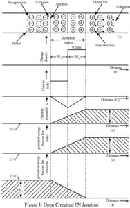
What is Open Circuit PN Diode? Figure 1(a) shows an open circuited pn diode with acceptor impurity density NA in the p-region and donor impurity density ND in the n-region. We assume that each acceptor atom has ionized resulting in one immobile negatively charged acceptor ion and one mobile hole. Similarly, each donor atom has ionized resulting in one immobile positively charged donor ion and one mobile electron. In Figure 1(a) the immobile acceptor ion is indicated by a minus sign enclosed within a circle while immobile donor ion is…
Read MoreTypes of PN Junction Diode
In this Tutorial we are describing PN diode and types of PN Junction Diode. What is PN Junction Diode? A PN junction or P-N diode consists of a semiconductor having two regions, a p-region and n-region with a junction in between. The junction region or the transition region where the nature of the semiconductor material changes from p-type to n-type is usually very thin, typically 10-6 to 10-4 cm wide depending on the method of concentration. What are the types of PN Junction Diode? Depending on the method of construction,…
Read MoreCommon Emitter Configuration of PNP Transistor
In the common-emitter configuration of PNP, the transistor emitter is the terminal common to both the input side and output side. The signal to be amplified is applied between base and emitter forming the input circuit while the amplified output voltage is developed across load impedance in the collector-to-emitter forming the output circuit. Figure 1 gives the basic circuit of a CE amplifier using load resistor RC. The Large Signal Current Gain | Common Emitter Configuration of PNP Transistor In a CB transistor, IE forms the input current while IC is…
Read MoreInput and Output Characteristic Curves of CB Transistor
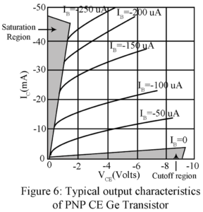
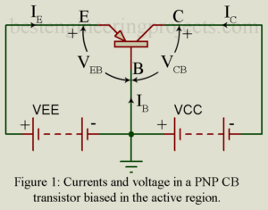
Here in this article we will going to discuss about characteristic curves of CB transistor like static input and static output characteristic curve of CB transistor (Common Base). Characteristic Curves of Transistor in Common Base Configuration Figure 1 shows a PNP transistor connected in Common Base (CB) configuration. Base is the terminal common to the input side and the output side and this terminal has been grounded. Then we are left with two voltage variables namely VEB and VCB. Further the current IB is ignored since it is nothing but…
Read MoreAmplifying Action of Transistor
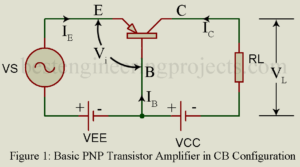
In this article you will learn about emitter efficiency, base transport factor, The early effect, dynamic emitter resistance and amplifier action of transistor. What do you mean by amplifying action of transistor? A transistor may serve various functions but basically it is used to amplify an electrical signal. Figure 1 gives the basic circuit of a PNP transistor amplifier in common base (CB) configuration. However, we may use an NPN transistor and get the same results. In figure 1, the transistor is biased for active region operation i.e. JE is…
Read MoreCurrent Components in a Transistor in Active Region Operation
Figure 1 shows the various current components in a pnp transistor operating in the active region. The entire emitter current IE consist of two parts (i) hole current IpE carried by holes diffusing across JE from p-type emitter to n-type base and (ii) electron current InE carried by electrons diffusion across JE from n-type base to p-type emitter. The ratio equals where and are respectively the conductivity of the p-type emitter region and n-type base region. Typically > . Hence in a pnp transistor, IpE>>Inr and hence we may neglect…
Read MoreTypes of Transistor on the Method of Construction
A bipolar junction transistor (BJT) forms an extension of a PN diode. It is three-layer semiconductor device with two junctions. Further it is a bipolar device i.e. the current is carried by two types of charge carriers namely electrons and holes and hence the device is called a Bipolar Junction Transistors. A BJT is basically used as an amplifier i.e. as a circuit for amplifying or increasing the magnitude of a periodic or an a-periodic voltage or current. A junction transistor may be of PNP type or NPN type and…
Read MoreCommon Drain Amplifier using FET
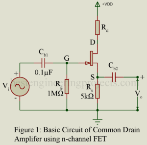
Common Drain Amplifier Introduction In the common drain amplifier, the input signal is applied between the gate and drain and the amplified output voltage is developed across a resistor in the source-to-drain circuit. The drain is the terminal common to the input and the output sides. Figure 1 gives the circuit of one stage of a common drain amplifier (CD) using n-channel FET. Rs is the load impedance placed in the source circuit. Quite often a resistor Rd is placed in the drain circuit to further stabilize the operation of…
Read MoreCommon Source Amplifier using FET
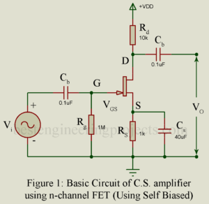
Common Source Amplifier In this amplifier, input signal is applied between gate and source and the amplified output voltage is developed across a load resistor in the drain circuit. Thus, source is the common terminal between the input side and the output side. Figure 1 gives the circuit of one stage of common source amplifier (CS) Amplifier using n-channel FET and with biasing arrangement. The typical component values are also shown in figure. This circuit is analogous to common emitter amplifier. On using p-channel FET, polarity of supply voltage is…
Read More
