Here in this article we will going to discuss about characteristic curves of CB transistor like static input and static output characteristic curve of CB transistor (Common Base).
Characteristic Curves of Transistor in Common Base Configuration
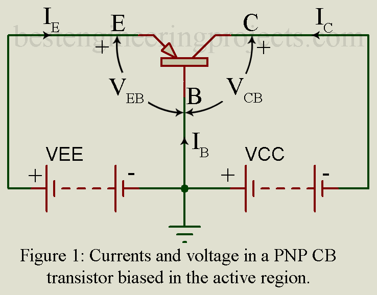
Figure 1 shows a PNP transistor connected in Common Base (CB) configuration. Base is the terminal common to the input side and the output side and this terminal has been grounded. Then we are left with two voltage variables namely VEB and VCB. Further the current IB is ignored since it is nothing but -(IE + IC). Then we are left with two current variables namely VEB, VCB, IE and IC any two may be selected as the independent variables and the other two as the dependent variables. In any transistor we select input current and output voltage as the independent variables and output current and input voltage as the dependent variables. Then, IC and VEB may be expressed in terms of VCB and IE as per following equation:
 ………..(1)
 ……….(2)
Hence, for a CB transistor we may be obtained the following two families of static characteristic curves plotting equations (1) and (2).
- Static output characteristic curves plotting equation (1). Thus, we plot IC against VCB with IE as parameter i.e. plot curves for different values of IE.
- Static input characteristic curves plotting equation (2). Thus, we plot VEB against IE with VCB as the parameter i.e. plot a set f curves for different values of VCB.
Circuit Setup | Input and Output Characteristic Curves of CB Transistor
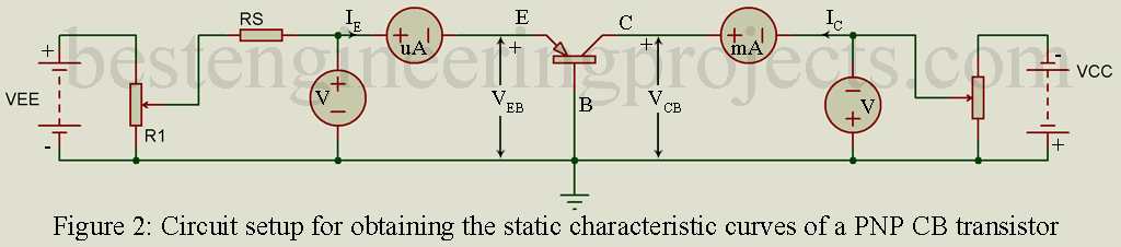
Figure 2 gives the basic circuit set up for determining the static characteristic curves of a PNP transistor. Current IE may be varied by potentiometer R1. But, VBE is low typically less than 1 volts. Hence, we include a series resistor RS (about 1 k-ohm) in the emitter circuit to keep IE low.
Voltage VCB may be varied by potentiometer R2. Millimeter and voltmeters are connected as shown in figure 2 to read I=E, IC, VEB and VCB.
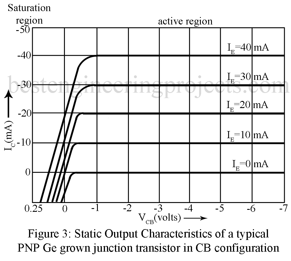
Static Output Characteristics of a PNP CB Transistor | Input and Output Characteristic Curves of CB Transistor
Figure 3 shows the static output characteristic curves of a typical PNP Ge grown junction transistor in CB configuration. Experimental procedure consists in setting upto circuit as shown in figure 2, fixing IE initially to zero, increasing the magnitude of VCB from zero in steps of say 1 volt, noting the corresponding IC and plotting IC against VCB. The procedure is repeated for higher values of IE say 10 mA, 20 mA etc. Thus, we get the curves shown in figure 3. In fact, these curves are nothing but plot of equation (2).
Active Region | Input and Output Characteristic Curves of CB Transistor:
For active region operation. JE is forward biased whereas JC is reverse biased. Consider the operation with IE = 0. Then, the transistor behaves as a reverse biased diode constituted by the order of microamperes in Ge transistor and nanoamperes in Si transistor. ICO remains constant for all value of collector voltage VCB below the breakdown potential. In pnp transistor, ICO flows from base to collector and hence is considered negative since assumed positive direction of ICO is taken to be the same as that of IC i.e. into the device. In npn transistor, ICO flows from collector to base and is, therefore, considered positive.
Next let a small emitter current IE (say 10 mA) flow in the emitter circuit. then a fraction  IE of this current reaches the collector and contributes
  IE to the total collector current IC as given by equation
 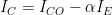 . In the active region, both components ICO and
  , collector current IC almost equals .
Output characteristics for IE = 20 mA, 30 mA etc. are similar to the characteristic for IE = 0 but shifted upward by . However, because of the Early effect, the output characteristics have a small upward slope. This slight upward slope of the output characteristic results in a finite output conductance instead of zero output conductance i.e. very large output resistance instead of finite output resistance.
Saturation Region | Input and Output Characteristic Curves of CB Transistor
In saturation region both JE and JC are forward biased. Hence, in pnp transistor, the saturation region lies to the left of ordinate VCB = 0 and above the characteristic for IE = 0. In this region, the voltage has dropped near the bottom of the characteristic with VCB = 0 and hence bottoming is said to take place. In a PNP transistor, VCB is actually slightly in this region i.e. JC is forward biased. Hence, collector current IC increases exponentially with VCB as per basic diode relationship. With JC forward biased, hole current flows from p-type collector region across JC to n-type base region. As a result, the net hole current magnitude drops rapidly as shown in figure 4. If the forward bias is JC is further increased, IC may even become positive.
Cutoff Region | Input and Output Characteristic Curves of CB Transistor
The output characteristics are almost parallel. But only the characteristic for IE = 0 passes through the origin. This output characteristic for IE = 0 does not coincide with the voltage axis. Rather IC equals ICO, a few  for Ge (Si) transistor. Since ICO is very small, the characteristic appears to coincide with the voltage axis. The region below and to the right of characteristic for IE = 0 is called the cutoff region and in the region both JE and JC are reverse biased.
Static Input Characteristic of CB Transistor | Input and Output Characteristic Curves of CB Transistor
Figure 4 gives the static input characteristic of a typical CB pnp Ge transistor. The experimental procedure consists in setting up the circuit as shown in figure 2, fixing VCB = 0, increasing the magnitude of IE from in steps of say 5mA, nothing the corresponding VEB and platting VEB against IE. the procedure is repeated for other values of VCB say -10 volts, -20 volts etc. and also with collector junction open. Thus, we get the curve shown in figure 4. In fact, these curves are nothing but plot of equation 2.

These input characteristics are simply the forward characteristics of JE for various values of VCB. Thus, with VCB open, the input characteristic is nothing but the forward characteristic of JE acting as a pn diode. With VCB = 0, i.e. with collector shorted to base, the collector sweeps away the minority carrier holes from base and the base therefore, attract more holes from the emitter. Hence, the characteristic for VCB = 0 is shifted downward relative to that for VCB open. The cut-in voltage VV is approximately 0.1-volt (0.5 volt) for Ge (Si) transistor for VCB = 0.
For a given value of VEB, any increases in |VCB|, as per Early effect, cause reduction in the effective base width, increases in the gradient of the minority carrier concentration in the base region and hence increases in IE. As a result, with increases of |VCB|, input characteristic curves shift downward as shown in figure 4.
It may be seen that a small increase in VEB causes large increases in IE. Thus, the dynamic input resistance  of CB transistor is quite low. This is true for both pnp and npn transistors.