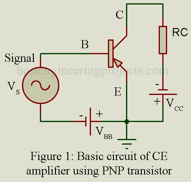
In the common-emitter configuration of PNP, the transistor emitter is the terminal common to both the input side and output side. The signal to be amplified is applied between base and emitter forming the input circuit while the amplified output voltage is developed across load impedance in the collector-to-emitter forming the output circuit.
Figure 1 gives the basic circuit of a CE amplifier using load resistor RC.
The Large Signal Current Gain  | Common Emitter Configuration of PNP Transistor
In a CB transistor, IE forms the input current while IC is the output current. The following equations relate the currents:
(1)
(2)
Combining equation 1 and 2 we get,
(3)
Equation 3 gives IC in terms of IB.
Let, (4)
Then, (5)
Let, (6)
Then equation (3) may be written as,
(7)
(8)
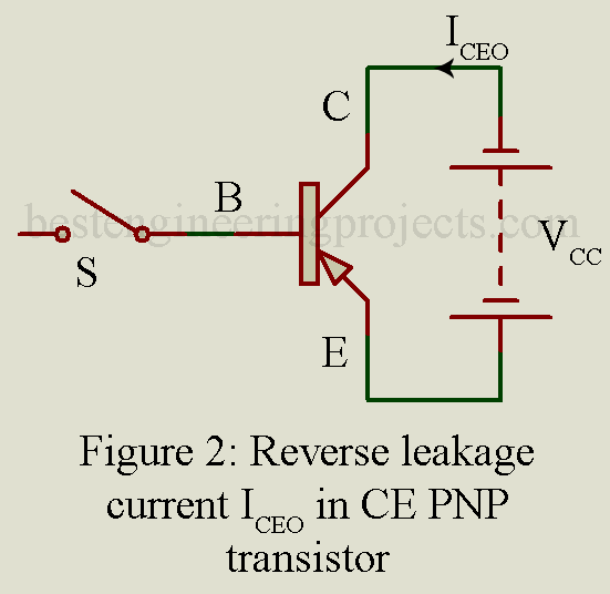
Figure (2) shows that in the CE transistor the output current IC equals input current IB multiplied by plus current ICEO. If IB is made zero i.e. base is open-circuited, then ICEO equals. This ICEO is the leakage current that flows between the collector and emitter with the base open as shown in figure (2).
From equation (6) it is equivalent that the magnitude of ICEO is much greater than that of ICO. Thus, with ,
so that ICEO is 100 times ICO in magnitude. In Si transistors, ICEO is a few microamperes while in Ge transistors, it is a few hundred microamperes. On rearranging equation (7) and replacing ICO with ICBO we get,
(9)
But CE cutoff condition is defined by IE = 0, IC = ICBO, and IB = -ICBO. Hence equation (9) states that equals the ratio of collector current increment from cutoff to the base current increment from the cutoff. Thus,
truly represents the large-signal current gain of a CE transistor.
(10)
Equation (10) states that is the ratio of the change in IC from cutoff to change in IB from cutoff.
DC Current Gain of CE Transistor  (or hFE) | Common Emitter Configuration of PNP Transistor
It is defined as the ratio of collector current to base current.
Thus, (11)
In general ICEO<< IC. Then, equation (10) yields .
Parameter hFE is a quantity of significance in the saturation region of the transistor and is usually provided in the manufacturer’s data, particularly for a switching transistor.
Small Signal Current gain  or hFE
At a given operating point or hFE is defined as the ratio of small collector current increment
to small base current increment
, keeping VCE constant.
Thus,
(12)
Static Characteristic Curves of a PNP CE Transistor | Common Emitter Configuration of PNP Transistor
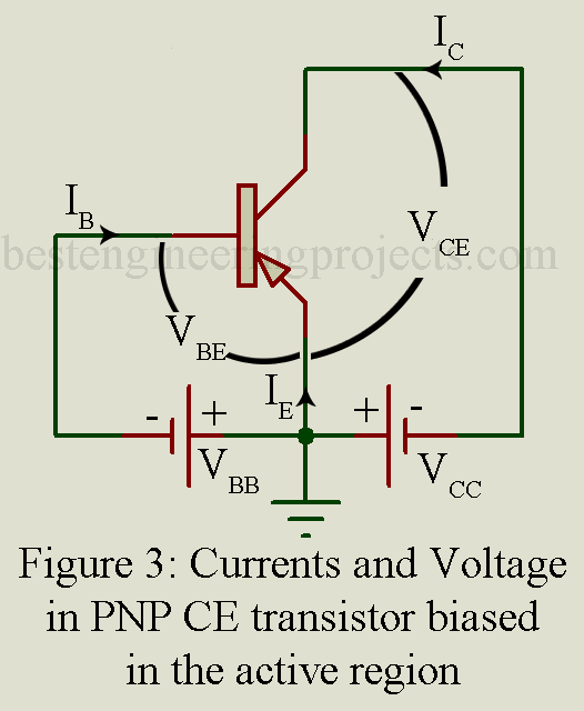
The CE configuration is the one most widely used in transistor circuits. Figure 3 shows a PNP transistor connected in a common emitter (CE) configuration. Here, the emitter is the terminal common to the input side and the output side, and this terminal have been grounded. Thus, we are left with two voltage variables namely VBE and VCE. Further, the current IE is ignoring, being equal to –(IC + IB). Thus, we are left with two current variables namely IB and IC. Out of these totals of four variables, the input current IB and the output voltage VCE are taken as the independent variables whereas the input voltage VBE and the output current IC form the dependent variables. Then IC and VBE be expressed in terms of VCE and IB as per the following equations.
(13)
(14)
When plotted equation (13) gives the static output characteristic curves while equation (14) gives the static input characteristic curves.
Circuit Setup of Common Emitter Configuration of PNP Transistor
Figure 4 shows the basic circuit arrangement for obtaining the static characteristics of a PNP transistor in CE configuration. For an NPN transistor, terminals of all batteries, milliammeters, and voltmeters have to be reversed. The base-to-emitter voltage VBE may be varied by potentiometer R1. Since this voltage VBE is quite low (less than 1 volt), we include a series resistor RS (typically 1 k-ohms) in the base-to-emitter circuit. This resistor helps in limiting the emitter current IB to a low value. The collector-to-emitter voltage VCE may be varied with the help of potentiometer R2. The milli-ammeters and voltmeters read IB, IC, VBE and VCE.
Static Input Characteristic Curves of CE Transistor | Common Emitter Configuration of PNP Transistor
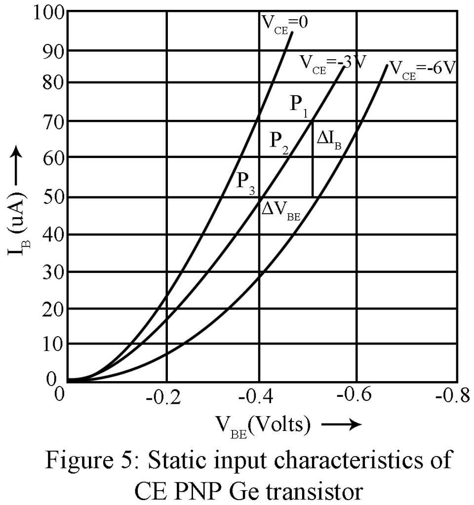
The experimental procedure for obtaining the static input characteristics consists in setting up to circuit as shown in figure (4), adjusting VCE to zero i.e. collector short-circuited to the emitter, increasing the magnitude of VBE from zero in regular steps of say -0.1 volt, noting the corresponding Ib and plotting Ib against VBE. The procedure is repeated for other values of VCE say -3-volt, -6-volt, etc. Thus, we get the input characteristic curves shown in figure (5).
The characteristic curves for VCE = 0 and width JE forward-biased are the same as for a forward-biased diode. If VBE is zero, IB almost becomes zero since now both emitter and collector junctions get short-circuited. For any nonzero value of VCE, the base current for VBE = 0 is not zero but is so small that it cannot be separately indicated in the figure (5). In general, constant VBE, as VCE increases, the base width decreases as per the Early effect and this, in turn, results in decreased recombination base current IB as shown in figure (5).
The static input characteristic curves for CE silicon transistors are similar to those in figure (5). However, the curves break away from zero current in the range of 0.5 to 0.6 volt instead of 0.1 to 0.2 volt as in the case of the Ge transistor.
The dynamic input resistance | Common Emitter Configuration of PNP Transistor
The dynamic input resistance of a transistor at given values of VBE and VCE is defined as the reciprocal of the slope of IB curves at that point and is given by,
(15)
Thus, consider the point P in figure 3.33 taken on the curve for VCE =-3 volts. At this point, and VBE = -0.5 volt. Consider the increment of IB from
to
. Considering
volt.
Then,
Static Output Characteristics of CE Transistor | Common Emitter Configuration of PNP Transistor
Equation (13) when plotted gives the static output characteristic curves. The experimental procedure consists in setting up the circuit as shown in figure (4) adjusting IB = 0, increasing the magnitude of VCE from zero in regular steps of say-2, nothing the corresponding IC, and plotting IC against VCE. The procedure is repeated for other value of IB say ,
etc. Thus, we get the static output characteristic curves shown in figure (6). These curves have shapes similar to the output characteristic in CB configuration but for the difference that in CE configuration the slopes of the curves are larger. Further, the output current i.e. collector current IC is much larger than the input current i.e. the base current, typically 100 to 200 times as large.
CE Active Region | Common Emitter Configuration of PNP Transistor
In the active region, JE is forward biased while JC is reverse biased. Hence, in Figure (6), the active region lies to the right of the ordinate VCE = a few tenths of a volt and above IB = 0 as shown. In the active region, the transistor responds more quickly to the input signal i.e. there are large changes in IC and VCE for any change in IB. For operation as a linear amplifier, the operation must be restricted to the active region.
We have seen that IC is given by,
………(16)
If is perfectly constant, then as per equation (16), IC will be independent of VCE and the curves in figure (6) will be horizontal. However, due to early effect, both
and
increases with increases of VCE. Thus, let increase in VCE cause 1% increases of
say from 0.98 to 0.99. Corresponding increases in
is from
i.e. from 49 to 99, and increases of 102%. Hence, there results in a high upward gradient in output characteristics in the CE circuit. This in turn results in low incremental output impedance r0 where r0 is given by,
(17)
Further from the figure (6), we find that the output characteristics start from the origin and do not enter the region of forwarding collector voltage. This results from the fact that JC is already forward biased by an amount of VBE when VCE reaches zero.
CE Cutoff Region | Common Emitter Configuration of PNP Transistor
The CE cutoff region is defined by IC = 0, IC = ICO and IB = -IC = -ICO and JE is reverse biased to about 0.1-volt (0 volt) for Ge (Si) transistor.
CE Saturation Region | Common Emitter Configuration of PNP Transistor
It is the region in which both JC and JE are forward biased by at least the cutin voltage.


