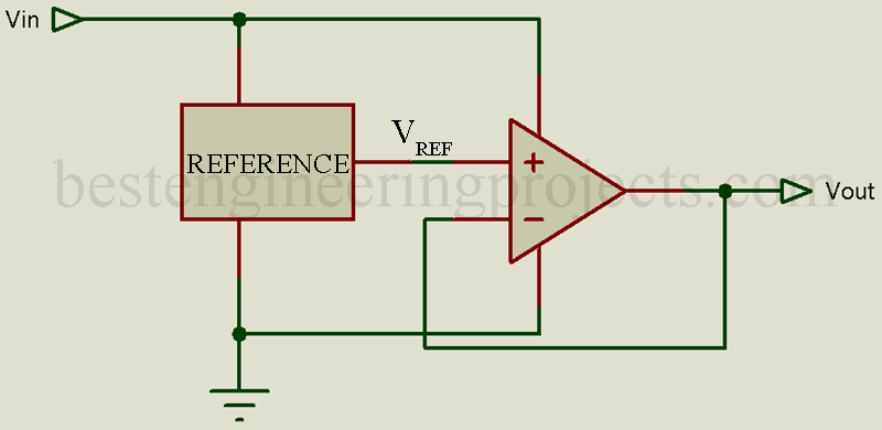
Voltage Regulator Description: IC Voltage regulators operates basically in the same manner as discrete circuit regulators. As illustrated in figure 1, the input voltage, usually the rectified ad filtered power-supply output, is applied to the reference circuit and to the op-amp. For optimum regulation, the op-amp must have high open-loop gain and a fairly large common-mode rejection ratio (CMMR).
The reference source determines the accuracy of the regulated voltage output. Reference voltages can be provided by such simple device as a zener diode or by more complex multi-transistor circuits, such as the ‘band gap’ voltage reference. Extremely stable reference circuits depend on automatic cancellation of drift characteristics due to temperature and input voltage changes.
Figure 1: IC Voltage Regulator with reference voltage and op-amp
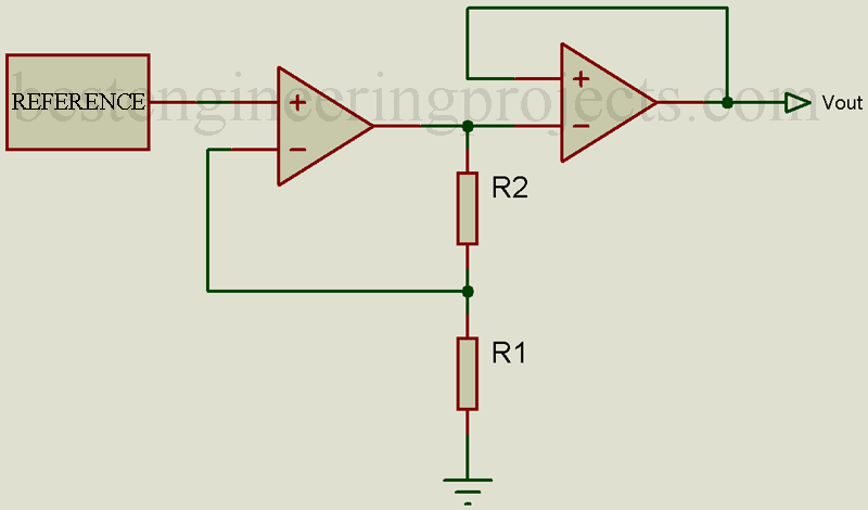
Figure 2 illustrates a method called “regulator within a regulator,” which is used in many IC voltage regulators to provide adjustment of the output voltage and, at the same time, reduce the output impedance of the regulator itself. In the circuit the output voltage of op amp (1) is determined by the ratio of R2/R1. The final output voltage V0 will be the reference voltage, modified by R2/R1 because the feedback factor of amplifier (2) is unity.
Figure 2: Regulator Within a Regulator
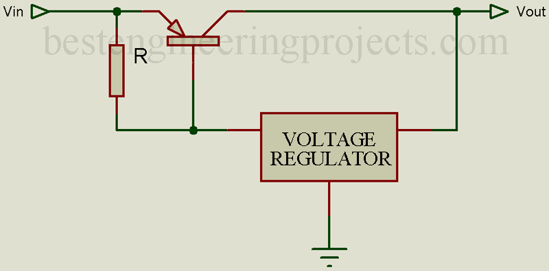
IC voltage regulators have a limited power-handling ability, and this can be expanded by using one or more external power transistors. The basic connection for a single external power transistor is shown in figure 3, but a variety of other connections Darlington pairs and parallel transistors can be controlled by the IC voltage regulator. Special features, such as automatic overload protection. Over-voltage protection, automatic thermal shut-down, short-circuit indication, remote control shut-down, etc., are available on different types of IC voltage regulators.

Key Parameters of Voltage Regulator
Output Voltage: The regulated output voltage maintained over specified operating range.
Input voltage: The range of input voltages for which the output voltage is maintained.
Line regulation: The change of output voltage for a corresponding change in input voltage.
Load Regulation: The change of output voltage for a corresponding change in output current.
Output voltage temperature coefficient: the change in output voltage per degree C change in junction temperature.
Output current range: Minimum output current required to maintained regulation and maximum output current.
Maximum operating junction temperature: Maximum temperature at which the IC voltage regulator con operate safely.
Maximum power dissipation: Maximum power that IC can dissipate at 250C (room temperature) without a heat sink of forced air cooling.
Maximum power dissipation: Maximum power that IC can dissipate at 250C (room temperature) without a heat sink or forced air cooling.
Safe operating area (SOA): A combination of maximum output current and the difference between input and output voltage. Usually the area under a curve that describes the maximum safe operating characteristics for different values of input and output voltage and maximum output current.
Applications
Wherever the power-supply must be kept at a fixed value, regardless of variations in load current or input voltage. Specific applications and part numbers will be discussed in following articles.
- Fixed Voltage Regulator
- Adjustable Output Voltage Regulator
- Tracking and Floating voltage Regulator
- Precision Voltage Regulator
- Switching Voltage Regulator
Comments
A wide variety of IC voltage regulators, with special features and many different characteristics, is available. Manufacturer’s specifications and application data should be studied carefully for special features, mounting instructions, external transistor connections, and thermal requirements. Switching regulators use entirely different operating principles and are described briefly in voltage switching regulators

