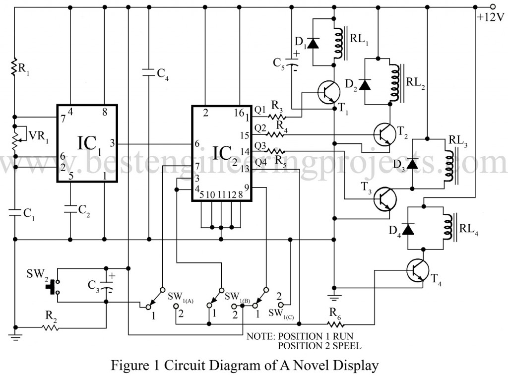
There are many display circuits already published in BEP. But the circuit Running and Spellar Effects of Light Circuit is very special in its own way because it contains all the facilities required for any type of decoration.
Lighting decoration broadly consists of two main categories-the running effect and the spellar effects. Running effect is well known to every electronics hobbyist. The spellar effect consists of many output driving the load-lamps; all of them go high one after another, and eventually all outputs becomes high simultaneously showing a complete display. Thereafter all the outputs go low and the cycle is repeated. Both these effects can be obtained by using thus circuit with just a flap of a switch!
As shown in the circuit, IC1 is wired as a free-running astable multivibrator whose frequency can be controlled through VR1. This changes the speed of running or spelling effect. The output of IC1 is directly connected to the clock input pin 6 of IC2 which is a CMOS shift register.
IF switch SW1 is kept in position 1, it connects pin 3 and 4 of IC2 to pin 12 of the same IC. Also, pin 9 is held high. So binary number 1000 is loaded in the register. This causes initially T1 to go high and T2, T3 and T4 low. Now as T4 is connected back to pin 3 and 4, the number 1000 is circulated continuously through the register in IC2 and as a result the four outputs sequentially go high. Thus a running effect is obtained.
Now keeping switch SW1 in position 2, pin 7 of IC2 is connected to pin 13. Pin 3 and 4 are held high and pin 9 is grounded. As pin 3 and 5 are high, all the outputs of IC2 go high one by one on each consecutive clock pulse. When T4 goes high, pin 7 of IC2 also goes high. This makes all the outputs low because all the parallel inputs are now grounded. Thus the operation repeats (ad infinity), and the spellar effect is obtained.
Check out other decoration project posted in bestengineeringprojects.com
- Christmas Music and Decoration using Arduino
- Christmas Decoration Circuit With Music
- Sequential Timer Circuit Using NE555
If more than four outputs are required, then more CD4035 (IC 2 ) can be cascade in the same fashion. Only their clock inputs should be driven from the same clock source in parallel.
The reset switch SW2 should be pushed on, in ‘run’ mode to bring all the outputs of IC2 low initially.
The output T1 to T4 of IC2 can be used to drive a general-purpose relay driver circuit. Since the circuit operates on +12V DC, any general-purpose power supply can be used to power the unit.
BEP LAB NOTE: It is advised that while changing switch SW1, power supply of the circuit should be kept off. However to avoid this problem, as IC2 is a CMOS IC, it can be replaced with TTL shift register IC 7495 by making minor modification in the circuit.
PARTS LIST OF RUNNING AND SPELLAR EFFECT OF LIGHT CIRCUIT
|
Resistor (all ¼-watt, ± 5% Carbon) |
|
R1 = 100 KΩ R2 = 1 KΩ R3 – R6 = 10 KΩ VR1 = 1MΩ LINEAR POT |
|
Capacitors |
|
C1, C4 = 0.1 µF (Ceramic Disc) C2 = 0.01 µF (Ceramic Disc) C3, C5 = 100 µF, 16V (Electrolytic capacitor) |
|
Semiconductors |
|
IC1 = NE555 (Timer IC) IC2 = CD4035 (CMOS Shift Register) T1 – T4 = BC147B (General purpose, Silicon NPN Transistor) D1 – D4 = 1N4001 (Rectifier Diode) |
|
Miscellaneous |
|
RL1 – RL4 = 12V, 100Ω Relays SW1 = position 1 run and position2 spell SW2 = Push-To-On switch |

Thanks you