Introduction | Load Protector Circuit and Remote Switching
Have you ever noticed the number of devices used at your house to serve your purpose? There are many. These devices require a specified rate of power to operate. Maximum variations in voltage/ power and load can destroy most of the devices like inverters and UPS systems since it can cause excessive heating of the output transformer windings and the active driving device and thereby damage them. And, some domestic appliances also need to be protected against under/over-voltage. This particular circuit serves the purpose. Named as the ‘Load Protector Circuit and Remote Switching’ circuit, it protects devices from fluctuations in the mains. Additionally, it also allows you to turn on/off the load through a remote handset. The main features of this circuit are briefed in points below:
Features of Load Protector Circuit and Remote Switching
1. It shuts down the load at under/over-voltage.
2. After under/over-voltage, the load is automatically restarted.
3. A visual indication is given for normal voltage, which goes off at under/over-voltage.
Circuit Description of Load Protector Circuit and Remote Switching:-
Figure.1 depicts the basic block diagram of the system that comprises a transformer, rectifier, filter, regulator, and comparator including remote switching transmitter and receiver circuitry. The remote signal transmitter aids the manual control of the device connected to the circuitry during normal conditions. Other components are set to automate the load-protecting operation.
The transformer steps down the AC mains which are then supplied to the comparator as well as the regulator after it is rectified and filtered through the system. The regulator generates a 12V power supply which is supplied to the entire circuit components except for the comparator and the timer.
Depending upon the function carried out, the circuit is sectioned into two parts- the transmitter and the receiver-cum-load protector.
The remote transmitter | Load Protector Circuit and Remote Switching
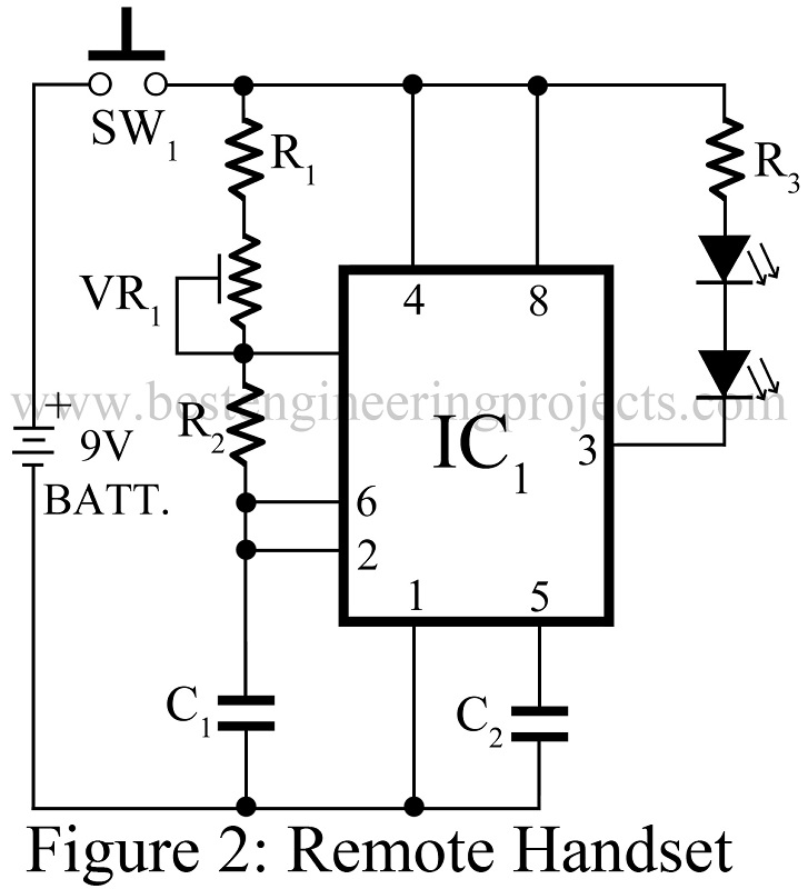
An astable multivibrator IC NE555 (IC1) builds up the remote handset which is powered by a 9V battery as shown in Fig.2. It also consists of a when the push-to-on switch (S1) which transmits a preset frequency once it is pressed. The remote transmitter transmits a preset frequency when push-to-on switch S1 is pressed. The modulated IR beam is received by phototransistor T1 of the receiver-cum-load protector unit.
The receiver-cum-load protector | Load Protector Circuit and Remote Switching
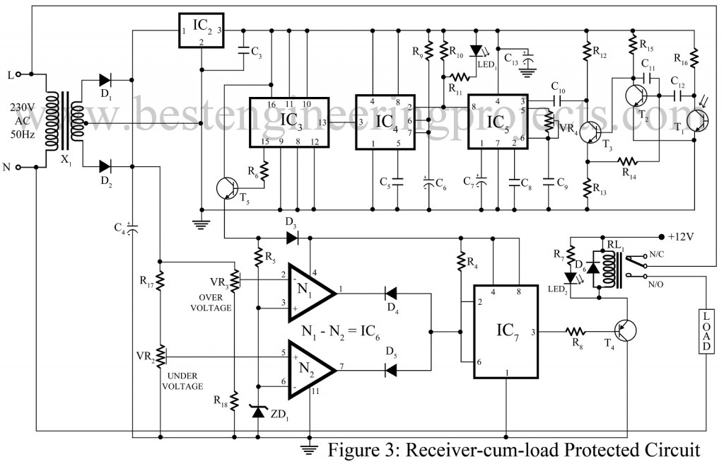
At the receiver side, the phototransistor T1 receives the modulated IR beam sent out by the transmitter as shown in Fig 3. Power supply, receiver, and protector sections are incorporated in this part.
Power supply | Load Protector Circuit and Remote Switching
The detailed figure of the circuit is illustrated in fig.3. Here the AC mains supply is used in two ways in this circuit- it is directly supplied to the circuit through fuse F1 and next, it is stepped down to produce a secondary output of 18V-0-18V, 250mA by a transformer X1. In the second case, the stepped-down voltage is again rectified and filtered by diodes D1-D2 and capacitors C1- C2 respectively. This output is then delivered to IC2, a junction that connects resistor R17 and preset VR3. At this point, IC2 generates 12V regulated output which is then smoothed by capacitor C3 and supplied to the circuit.
Receiver Section of Load Protected Circuit and Remote Switching.
The receiver section covers the top right corner of the circuit comprising components from IC3 to IC5 and transistor T1 to T3 configured in Darlington-pair mode. Since transistor T1 is sensitive to infrared signals, it is used to sense those signals. The reception of incident photons generates the base current. The current produced is so small that a gain of T1 is used to amplify the current.
The photo-transistor (T1), supplies the frequency signals to the NPN transistors T2 and T3.
After being amplified by the transistor pair (T2 & T3), these signals are applied to the phase-locked loop IC-NE567 (IC5) through capacitor C10. IC5 used here is a highly stable phase-locked loop with synchronous AM lock detection and power output circuitry. This IC is mostly used to drive a load whenever a sustained frequency falling within its detection band is present at its self-biased input, i.e. used as a tone decoder. Few external components predict the values of the center frequency of the band and the output delay separately.
The primary function of IC5 is to detect the code frequency. The input signal sets the center frequency of the current-controlled oscillator. But, when no input is given, a combination of preset VR4 and capacitor C9 is employed to detect the frequency of the internal free-running oscillator. Preset VR4 sets the center frequency of the IC5 as required, in the code frequency range. This frequency must match the frequency of the code generator in the transmitter section. Capacitor C7 and C8 are used to attenuate frequencies outside the detection band to avoid forged outputs and determine the low-pass frequency respectively.
As long as the transmitted code frequency is detected by the IC5, it produces low output at pin 8. This situation is assured by the glowing LED1. The low output of IC5 functions as a triggering input to a monostable multivibrator IC4. The time period of this IC is approximately 1 second. The JK flip-flop IC CD4027 (IC3) is wired in a toggle configuration. It gets activated by the clock signal fed by the IC4 through pin 13 of the IC3.
The output of the IC3 (pin 15) goes high as it receives the first clock signal. It goes low on the next clock signal. Transistor T5 collects the IC3 output through resistor R6 and only when output is high, it provides the supply to the comparator IC6 and timer IC7.
Load protector | Load Protector Circuit and Remote Switching
The leftmost part of the circuit performs the function of load protection. This unit comprises diodes; D1 and D2, comparator IC6, and timer IC7. The operational amplifier IC LM324 is what builds up the comparator. The comparator consists of two frequency-compensated operational amplifiers which exhibit high gain properties. These amplifiers operate from a single supply and therefore receive supply from the reference voltage (6.2W) generated and stabilized by the combination of resistor R5 and Zener diode ZD1 through the respective pins; non-inverting pin 3 of N1 and inverting pin 6 of N2.
As clearly shown in the figure, preset VR2 and VR3 are inserted in pin 2 and 5 of the amplifiers; N1 and N2 to set the over-voltage and under-voltage conditions.
The resistor R4 always maintains pin 2 and 6 of IC7 in the high state. During over/under-voltage conditions, when the output of anyone comparator either N1 or N2 goes low, the output coupled to pin 2 of IC7 through diodes D4 and D5 configured as wired-OR operators, goes low. It triggers the IC and the output pin 3 of IC7 goes high and cuts off transistor T4 which in turn de-energizes the relay RL1.
We can observe here IC7 (NE555) carries out a level sensing function, during a normal voltage situation, it drives PNP transistor T4 into conduction that energizes the relay RL1 to operate the device connected at its terminal smoothly. And, when voltage variations are likely to affect the device, it de-energizes relay to prevent damage to the connected appliances. Additional components like diode; D6 and LED2 are used as a freewheeling diode and for indication of relay energization respectively.
Construction of Load Protector Circuit and Remote Switching
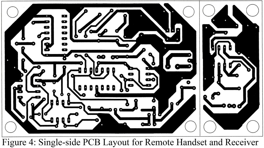
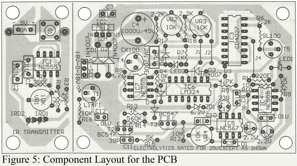
The fact that it can be assembled on any general-purpose PCB is another useful feature of this project. The definite size of the PCB design along with single-side combined PCB layout for the remote handset (Fig.2) and the receiver cum-load protector (Fig. 3) is shown in Fig. 4 and its component layout is given in Fig.5.
It is highly recommended to use IC bases instead of directly soldering the ICs onto the PCB so that the problems of components damage can be set aside. To achieve 100% benefits from this project, proper contacts must be established between the pins of the IC bases and the solder points on the PCB.
Working of Load Protected Circuit and Remote Switching
This circuit works on three different conditions:
Normal condition-
For normal ac supply (200W-245W), the output of IC2 is low which energises the relay through PNP transistor T5 and the adequate supply to the load connected at the relay terminal is provided.
Over-load condition-
As the mains exceed 245V, the sampled voltage at pin2 turns higher than the reference voltage (6.2v), the output of amplifier N1 at pin 1 goes low. It triggers the IC7 and the output of IC7 goes high causing the PNP transistor (T4) to cut off and de-energize the relay. When the relay stops working, the appliances stop operating and the LED1 stops glowing to notify about the scenario.
Under-load condition-
In the same way, when ac supply falls below rated voltage .i.e. below 200V, the voltage rating at pin 5 goes low than the reference voltage (6.2V). Corresponding to this, the output at pin 7 of amplifier N2 goes low and triggers the IC7. The IC7 then supplies a high output to the relay and de-energizes it. In this state, the LED1 stops glowing to indicate that there is variation in supply and the appliances are protected.
Remote switching of the load
The circuit offers an extra facility with the fact that it allows remote switching control of the appliances during normal conditions. For this additional feature, all we need is a simple switch connected across the relay. During normal ac supply, the appliances operate smoothly. During this, the normally opened contacts (N/O) of relay RL1 are in ‘on’ condition. In order to stop the device from working, we have to break the connection. Pressing switch S1 for a few seconds solves that problem. Once the switch is pressed, pin 15 of IC3 goes low. This blocks the supply to IC6 and IC7. Hence, the relay RL1 de-energizes and breaks the connection between load and supply which prevents the device from working.
If the switch S1 is pressed again, it toggles IC3 and re-establishes the connection, IC6 and IC7 receive supply from IC3 and the relay is energized. This process goes on and on for countless switch pressing activities. The remote transmitter can work efficiently within a distance of up to 8 meters from the load.
PARTS LIST OF LOAD PROTECTED CIRCUIT AND REMOTE SWITCHING
| Resistor (all ¼-watt, ± 5% Carbon) |
| R1, R5, R8 = 4.7 KΩ R2 = 390 Ω R3 = 47 Ω R4, R10, R12, R16 = 10 KΩ R6, R17, R18 = 2.2 KΩ R7, R13 = 1 KΩ R9 = 470 KΩ R11 = 220 Ω R14 = 560 KΩ R15 = 5 KΩ VR1 – VR4 = 10 KΩ Preset |
| Capacitors |
| C1, C2, C5, C9, C12 = 0.01µF (Ceramic Disc) C3, C8, C10 = 0.1µF (Ceramic Disc) C4 = 1000µF/25V (Electrolytic) C6, C7 = 2.2µF/25V (Electrolytic) C11 = 39 Pf (Ceramic Disc) C13 = 33µF/25V (Electrolytic) |
| Semiconductor |
| IC1, IC4, IC7 = NE555 Timer IC IC2 = 7812, 12V Voltage regulator IC3 = CD4027 Dual J-K flip-flip IC5 = NE567 Phase-lock loop IC6 = LM324 Comparator ZD1 = 6.2V Zener Diode D1 – D3 = 1N4007 Rectifier Diode D4, D5 = 1N4148 Switching Diode T1 = L14F1 Phototransistor T2, T3 = BC547 NPN transistor T4 = CK100 PNP transistor T5 = SL100 NPN transistor IRD1, IRD2 = Infrared diode/LED LED1, LED2 = Red LED |
| Miscellaneous |
| RL1 = 12V, 200Ω 1C/O relay X1 = 230V AC to 18-0-18V, 250mA secondary transformer |


Great works