Pulse Width Modulation (PWM) is a technique to control the average power delivered to the analog devices. With an acquisition of 555 IC amongst most people working with electronic devices, the use of 565 IC is like using two 555 ICs inside a single device. Unlike 555 IC, 565 IC has 14 pins which act as a dual timer. 565 IC is also available with 10 pins. Nevertheless, they both require the same amount of power supply.
PWM using 565 IC is a form of Pulse Time Modulation (PTM), also known as Pulse Duration Modulation (PDM) and Pulse Length Modulation (PLM). A simple means of PWM generation is shown in figure 1 using 565 PLL. It actually creates a Pulse Position Modulation (PPM) at a VCO output (pin 4), but by applying it and the input pulses to an Exclusive OR gate, PWM is also created.
Circuit Description of Pulse Width Modulation using 565 IC
The 565 timers, a very popular Phase Locked Loop (PLL) unit, contain a phase comparator (PC), amplifier, low pass filter, and Voltage Controlled Oscillator (VCO). PC, VCO, and amplifier are connected internally. The circuit in Figure 1 has a 10-pin 565 IC, a general-purpose amplifier transistor, and an Exclusive-OR 2 input 7486 IC which has 14 pins. Not to mention, the circuit has a number of resistors and capacitors. An external resistor and capacitor are for setting free-running or center frequency of VCO and another external capacitor is for setting low-pass filter passband. The input signal is given to both the ICs, yet the PWM output and the PPM output are given by the 7486 IC, which is an advanced CMOS with high-speed functionality. The VCO output is connected back as the input to the PC so as to close the PLL loop.
For the PLL to remain locked, its VCO input (pin 7) must remain constant. The presence of an external modulating signal upsets the equilibrium. This causes the phase detector output to fluctuate: either go up or down, to maintain the VCO input (control) voltage. However, a change in phase detector output also means a change in phase difference between the input signal and the VCO signal.
Thus, the VCO output has a phase shift proportional to the modulating signal amplitude. The PPM output is amplified by transistor T1 in figure 1 just prior to the output. The Exclusive-OR circuit provides a “high” output only when just one of its two inputs is “high”. Any other input condition produces a “low” output. By comparing the PPM signal and the original pulse input signal as inputs to the Exclusive-OR circuit, the output is a PWM signal at twice the frequency of the original input pulses.
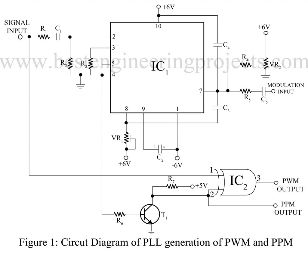
Adjustment of VR1 varies the center frequency of the VCO. The VR1 potentiometer may be adjusted to set up the quiescent PWM duty cycle. The output (PPM or PWM) of this circuit may then be used to modulate a carrier for subsequent transmission.
From controlling the CPU fans to dimming the LED lights, the Pulse Width Modulation technique is used in quite a number of places. With efficiency being high, lower loss in power, and its ability to control the delivered power with good precision, PWM is being used over conventional techniques. With alterations made with the pulse width of control signals, the power being delivered to load can be controlled.
Check out more projects related to pulse width modulation.
- PWM Generator and Class D Power Amplifier
- Frequency Shift Keying (FSK) Generator Using PLL 565
- Low Frequency Sine Wave Synthesizer
- Speech Communication using Laser
PARTS LIST OF PHASE LOCKED LOOP USING 565 IC
| Resistor (all ¼-watt, ± 5% Carbon) |
| R1 = 33 KΩ
R2, R3 = 390 Ω R4 = 4.7 KΩ R5 = 5.6 KΩ R6 = 10 KΩ R7 = 5 KΩ VR1 = 6 KΩ VR2 = 10 KΩ |
| Capacitors |
| C1 = 0.1 µF (Ceramic Disc)
C2 = 1000 pF (Ceramic Disc) C3 = 0.001 µF (Ceramic Disc) C4 = 0.01 µF (Ceramic Disc) |
| Semiconductors |
| IC1 = 565 (PLL IC)
IC2 = 7486 (exclusive or gate) T1 = 2N4123 (General Purpose Amplifier Transistor) |
Updated on 3rd August 2020