Introduction to Field Effect Transistor (FET)
A Field Effect Transistor (FET) is a transistor in which current is controlled by an electric field. A conventional transistor is a bipolar device i.e. current is carried by two types of charge carriers namely electrons and holes. Hence a conventional transistor is referred to as a Bipolar Junction Transistor (BJT). An FET, on the other hand, is a unipolar device i.e. current is carried by only one types of charge carrier namely the majority carriers.
What are the Advantage of Field Effect Transistor (FETs) over BJTs
- Higher input impedance (Several M-ohms)
- Lesser noise, being a unipolar device
- No offset voltage at zero output current. Hence FET forms an excellent chopper
- Relatively less effected by radiation
- Better thermal stability
- Simpler to fabricate in IC form and lesser space requirement
Drawback of FETs:
Relatively small gain-bandwidth product
What are the Types of Field Effect Transistor (FETs)
FETs may be of the following two types:
- Junction Field Effect Transistors (JFET or Simply FET)
- Insulated get FET (IGFET), also called Metal-oxide Semiconductor FET (MOST or MOSFET)
MOSFETs are superior to JFETs in several respects and are, therefore, popularly used.
Introduction to Junction Field Effect Transistor (JFET)
Figure 1 shows the basic structure of an n-channel FET. It consists of (a) n-type semiconductor bar which forms the channel (b) two heavily doped p-regions formed by alloying of diffusion on two sides of the bar (c) ohmic contacts at the two ends of the bar (d) leads connected to the ohmic contact and the two p-type regions.
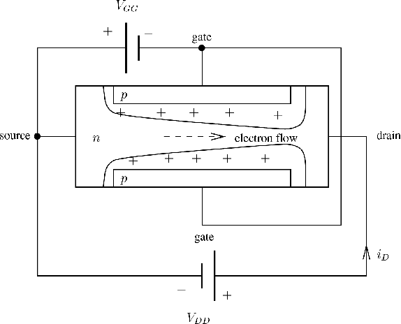
Figure 1: Basic Structure of Junction Field Effect Transistor (JFET)
The n-type bar in between the two heavily doped p-regions forms an n-channel through which current flows from one end (say the left-hand end) called the source to the other end (the right-hand end) called the drain. The current is carried by the majority carriers, electrons in the case of n-channel FET and holes in the case of p-channel FET.
Source: The source is the terminal (taken as the left-hand terminal in figure 1) through which the majority carriers enter the bar driven by the eternal bias. The conventional electric current entering the channel at source S constitutes the source current Is.
Drain: The drain is the terminal (taken as the right-hand terminal in figure 1) through which the majority carriers leaves the bar. The conventional electric current entering the channel at drain D constitutes the drain current ID. Symbol VDS stands for the drain-to-source voltage. Voltage VDD indicates the drain supply voltage. In figure 1, VDS = VDD.
Gate: The gate G is constituting by two heavily doped p-regions placed on the upper and lower sides of the n-type bar formed by allowing, by diffusion or by some other method. A d.c. voltage VGS (=-VGG) is applied between the gate and the source to reverse bias the gate-to-source junction. In the n-channel FET of Figure 1, the gate is given negative voltage with respect to the source as well as the drain. The conventional electric current entering the bar at gate G constitutes the gate current IG.
Channel: This is the portion of the n-type bar between the two gate regions through which the majority carriers move from the source S to drain D.
Corresponding with BJT The source, gate and drain of an FET correspond to the emitter, base and collector respectively of a BJT.
Circuit Symbol and Polarity Convention of Junction Field Effect Transistor (JFET)
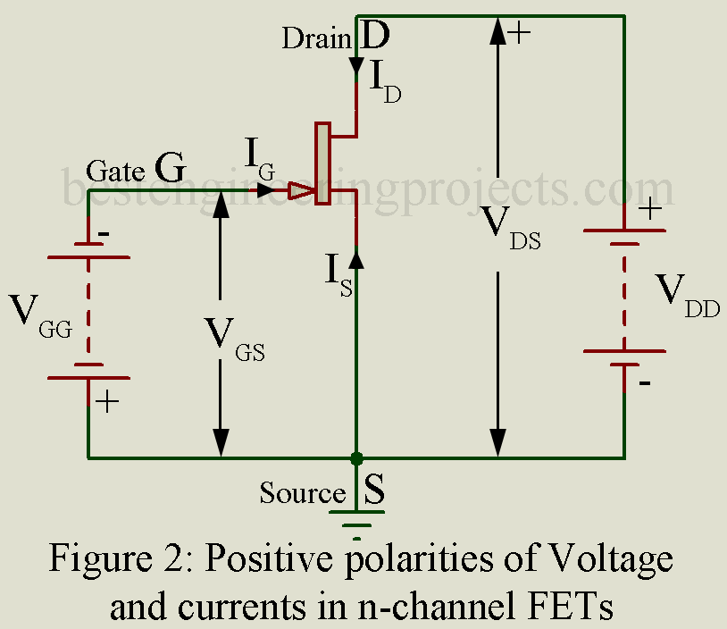
Figure 2 shows the circuit symbol for an n-channel FET. The direction of arrow at the gate in the symbol of FET gives the direction in which the gate current flows with gate junction forward biased. Thus, in the n-channel FET of figure 2, the arrow points into the device. Figure 2 also shows the supply voltages VDD and VGG for proper biasing. The assumed positive direction of all the three currents namely source current IS, gate current IG and drain current ID are into the device.
Thus, for the n-channel FET of Figure 2, ID is positive while IS is negative. Figure 2 also shows the polarities of voltage VGS and VDS. Thus, plus sign (or a dot) at one end gives the assumed positive polarity. Thus, VDS indicates the voltage of drain D with respect to source S. It drains is actually positive with respect to the source, then VDS is positive. Thus, in figure 2, VDS is positive while VGS is negative.
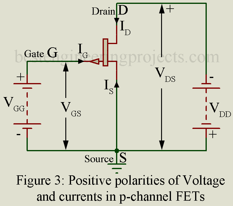
Figure 3 shows the circuit symbol for a p-channel FET. It also gives the supply voltage VDD and VGG for proper biasing. In the circuit symbol for FET, the arrow at the gate points away from the device giving the direction in which the gate current flows if gate is given a forward bias. For p-channel FET, ID and VDS are negative while VGS is positive.
Working of an n-channel Field Effect Transistor (FET)
In a n-channel FET of figure 1, the gate-t-channel junction is reverse biased. But the p-type gate region is heavily doped while the n-type channel region is lightly doped. Hence, the depletion region extends only slightly into the gate region but extends deeply into the channel region reducing effective conducting cross-sectional area. This reduced effective cross-sectional area of the channel reduces the overall channel conductivity and hence reduces the current flow from source to drain. As the reverse bias at the gate increases, the drain current ID reduces.
Thus, for a fixed VDS, we may control the drain current ID by varying the magnitude of the reverse bias at the gate junction. Any time varying voltage Vgs applied in series with the reverse gate bias voltage VGS results in corresponding time-varying component id in drain current. The current id following through the load resistor RL in the drain circuit produces corresponding time varying voltage id.RL across the load resistor RL. This voltage id.RL forms an amplified version of the signal voltage Vgs applied in the gate circuit.
Why the name Field Effect Transistor
This transistor is called Field Effect Transistor because the control of output current (drain current) is the effect of the extension of the field associated with the depletion region caused by the reverse bias at the gate.
Static Characteristic Curves of Field Effect Transistor (FET)
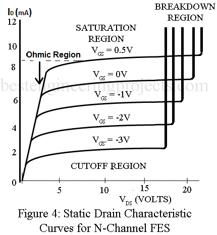
Figure 4 gives the static drain current ID versus drain-to-source voltage VDS characteristics of a typical n-channel FET in common source configuration. In figure 4, drain current ID is plotted against drain-to source voltage VDS with gate-to-source voltage VGS as the parameter. Let us first consider the characteristic for VGS = 0 i.e. with zero bias at the gate. Then the channel is fully open. Under this condition, with VDS = 0, there is no field attracting the majority carrier electrons to the drain terminal. Hence, in spite of full open channel, the majority carriers do not go to the drain and the drain current ID is zero. Now the n-channel, being a semiconductor, follow Ohm’s law.
Hence, on application of a voltage VDS, current ID is proportional to VDS in the region OA in figure 4. But the current ID causes ohmic voltage drop in the channel which reverse biases the gate junction resulting in narrowing of the channel is not uniform along the length of the channel. The narrowing is more at distance further from the source as shown in figure 1. As the magnitude of VDS increases, at critical value of VDS, channel gets pinched off i.e. more or less blocked and all the charges from the channel at the section get removed. This value of VDS is called pinch off voltage Vp. For VDS > VP, current ID remains almost constant. Figure 4 shows that this pinch off is not sharp but gradual. Further at pinch off, the channel does not get fully closed and ID does not reduce to zero but assumes an almost constant value. Had the channel gone fully blocked, ID would have reduced to zero and ohmic voltage drop in the channel would have reduced to zero. In that case, there would be no reverse bias producing the blocking of the channel.
With VGS negative, say -1 volt, the reverse bias gets increased and the pinch off voltage VP gets reduced. Further the saturation drain current is smaller. Characteristic curves for VGS = -2 Volts and -3 volts etc. are similar but VP and saturation current are reduced as shown in figure 4. For VGS = + 0.5-volt, VP and saturation current are higher than for VGS = 0. For silicon FET, Vv exceeds + 0.5 volts. Hence, with VGS = + 0.5-volt, gate current remains extremely small.
Avalanche Breakdown of Junction Field Effect Transistor (JFET)
As VDS is continuously increased, avalanche breakdown takes place and then ID suddenly increases to a high value. As the magnitude of reverse bias VGS is increased, avalanche breakdown takes place at reduced value of |VDS| as shown in figure 4. This result because the reverse gate added to the drain voltage VDS thereby increasing the effective voltage obtainable across the gate junction. Thus, the maximum permissible VDS is the lowest voltage which causes avalanche breakdown.
Commercial FET Structure
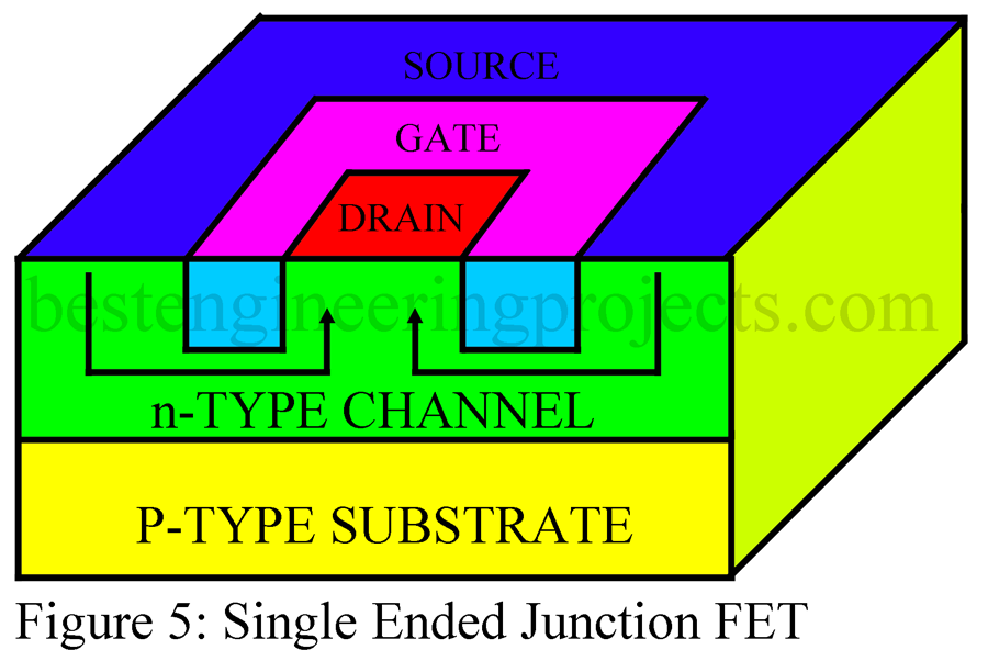
The FET structure shown in figure 1 is not popularly used commercially because it involves diffusion of impurities on both sides of the semiconductor wafer. Figure 5 shows the basic structure of a commercial FET. It is a single-ended geometry junction FET utilizing diffusion on one side only. It uses a p-type substrate on which n-type channel is epitaxially grown. Subsequently a p-type gate is diffused into the n-type channel. The substrate serves as the second gate. Both the p-type diffused gate and p-type substrate serving as the gate are of low resistivity material so that the delectation region penetrates mostly into the n-type channel. Drain current follows a path as shown in figure 5.
