Introduction to Power Supply for Electronics Systems
A power supply plays a crucial role in the functioning of electronic systems. Most digital integrated circuits (ICs) require a ±5V supply, while linear ICs such as op-amps and special-purpose ICs need ±15V supplies. In this article, we will discuss a power supply that provides ±5V and ±15V outputs.
The Power Supply Circuit:
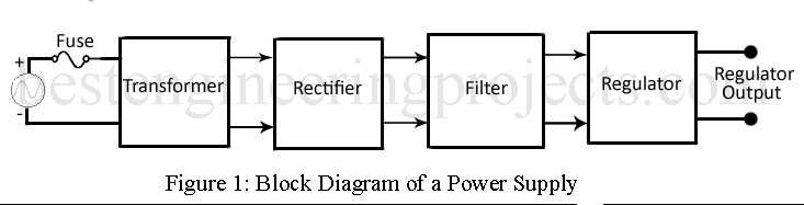
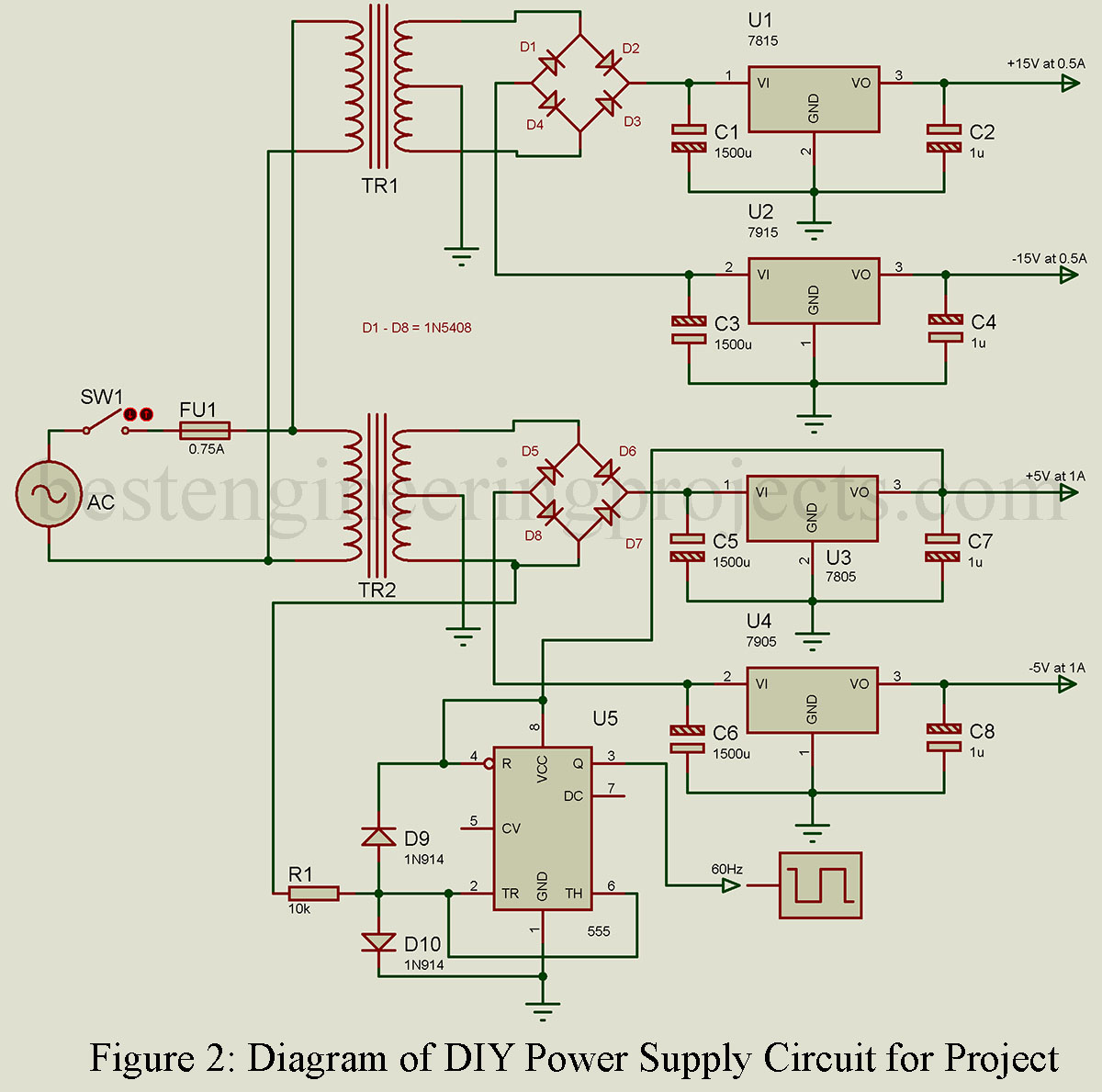
The block diagram of a typical power supply is illustrated in Figure 1. Figure 2 presents the schematic diagram of the power supply, designed to deliver an output voltage of ±5V at 1.0A and ±15V at 0.500A. In this configuration, two separate transformers are employed due to their easy availability. However, it is also feasible to create a single custom-designed transformer that meets the required specifications, thereby replacing the two individual transformers.
The supply voltages are derived from a center-tapped (CT) transformer with a rating of 26.8V, as well as a 12.6V CT transformer. These secondary voltages are then directed to the bridge rectifiers, which efficiently convert the sinusoidal inputs into full-wave rectified outputs. At the output of the bridge rectifiers, filter capacitors are employed to store the peak value of the rectified voltage whenever the diodes are in the forward-biased state. As the diodes do not remain forward-biased throughout the entire positive and negative half-cycle of the input waveform, the voltage across the filter capacitors exhibits a pulsating DC nature, comprising a combination of a steady DC component and a ripple voltage. To extract a regulated DC voltage, a regulator IC is employed, utilizing the pulsating DC voltage as its input.
Obtaining ±15V Supply Voltages:
Let’s delve into the process of obtaining the ±15V supply voltages in the circuit depicted in Figure 2. We have two regulators, namely the 7815 (+15V regulator) and the 7915 (-15V regulator), both capable of delivering output currents surpassing 1.0A. In Figure 2, these regulators effectively provide ±15V at 0.500A. However, it’s crucial to account for the dropout voltage (Vin – V0) of 2V. To ensure proper operation, the input voltage for the 7815 should be at least +17V, and for the 7915, it should be at least -17V. Consequently, the rectified peak voltage must exceed +17V and -17V, indicating that the secondary voltage needs to be higher than the 34V peak or 24V RMS. In the configuration shown in Figure 2, the center-tapped secondary voltage measures 26.8V RMS, thereby meeting the minimum requirement of 24V RMS. Additionally, the peak voltage between either of the secondary terminals and the center tap (ground terminal) amounts to 18.95V peak, which falls within the allowable maximum peak voltages of +35V and -35V for the 7815 and 7915 regulators, respectively.
It’s important to note that the voltages across the two halves of the center-tapped secondary exhibit equal amplitude but opposite phases. In the positive half-cycle of the input voltage, diode D1 conducts, causing capacitor C1 to charge towards a positive peak value of 18.95V. Simultaneously, diode D3 also conducts, resulting in capacitor C3 charging towards a negative peak value of -18.95V. Consequently, the voltage across the nonconducting diodes, D2 and D4, amounts to a 37.90V peak. This indicates that the bridge rectifiers’ peak-reverse-voltage (PRV) rating must exceed 37.90V peak or 26.8V RMS. The data sheets specify the PRV rating, also known as the working inverse voltage (WIV), for the bridge rectifier diodes. In the illustrated circuit (Figure 2), the MDA200 bridge rectifier from Motorola is utilized, which possesses a PRV rating of 50V, exceeding the necessary requirements. This particular bridge rectifier is chosen due to its availability and widespread usage.
During the negative half-cycle of the input waveform, diodes D2 and D4 become conductive, leading to the charging of capacitors C1 and C3 towards the peak voltage of 18.95V, following the indicated polarities. It’s worth noting that the diode pair conducting during either the positive or negative half-cycle does not remain conductive throughout the entire half-cycle. These diodes conduct only when the anodes are positively charged compared to the cathodes. This means that the capacitors are charged through current pulses when the diodes are forward-biased. The datasheets provide information on the maximum average rectified current, denoted as I0max, that the diode can safely handle. In the case of the MDA200, I0max is specified as 2.0A. Additionally, when the power supply is turned on, the capacitor’s initial charging generates a significant transient current known as the surge current, which passes through the diodes. This surge current, denoted as IFS, only flows briefly and is much greater than the maximum average current, I0max. The maximum surge current, IFSM, is typically listed on the datasheets, and for the MDA200, it is specified as 60A.
The secondary current rating of the transformer determines the selection of the filter capacitor size. As a general guideline, it is recommended to use a 1500-µF capacitor for every ampere of current. On the other hand, the working voltage rating (WVDC) of the capacitor depends on the peak rectified output voltage and should be at least 20% higher than the peak value of the voltage it is intended to charge to. Capacitors C1 and C3 in Figure 2 meet these criteria. Additionally, capacitors C2 and C4, situated at the output of the 7815 and 7915 regulators respectively, aid in enhancing the transient response and should fall within the range of 1µF.
Now let’s shift our attention to the ±5-V supply. Although the circuit configuration of the ±5-V supply is similar to that of the ±15-V supply, the transformer TR2 secondary specifications differ in this case. Consequently, the operation and considerations for the ±5-V supply mirror those discussed for the ±15-V supply.
It is important to note that the voltage regulators depicted in Figure 2 necessitate the use of heat sinks. Let’s explore the reasoning behind this requirement. The power dissipated by the 15-V regulators can be calculated as follows:
Power dissipated = (dropout voltage)(current)
= (18.95 — I5)(0.5) = 1.98 W
Similarly, the power dissipated by the 5-V regulators is
(8.91 – 5)(1.0) = 3.91 W
To ensure optimal performance, it is essential to employ proper heatsinking for the regulators, effectively managing their temperature. In the case of regulators with a metal package (such as the TO-3 type), a suitable heatsink is mounted on the package itself. However, for regulators with an epoxy package, silicon grease can be applied to the back of the package. Subsequently, the package can be securely fastened to the power supply cabinet’s chassis using insulating hardware.
In addition to the regulated supply voltages of ±15 V and ±5 V, there is often a requirement for a 60 Hz square-wave signal. This signal serves as a time base for scanning digital displays and acts as a trigger for sequential and timing circuits. If necessary, a 1 Hz (1 s) signal for a real-time clock can be easily derived from the 60 Hz signal using a divide-by-60 network. While less common, it is also possible to obtain a higher-frequency signal from the 60 Hz signal through the utilization of a multiplier. Figure 2 demonstrates the generation of a 60 Hz square-wave signal employing two small-signal diodes and a 555 timer functioning as the Schmitt trigger.
Conclusion:
A reliable power supply is essential for electronic systems. By following the circuit design and considerations discussed in this article, you can build a power supply that meets the voltage requirements of your project. Remember to use appropriate transformers, rectifiers, capacitors, voltage regulators, and heat sinks for optimal performance and safety.
Component List of Power Supply for Electronics Systems
Resistors (all ¼-watt, ± 5% Carbon)
R1 = 10 kΩ
Capacitors
C1, C3 = 1500 µF
C2, C4, C7, C8 = 1 µF
C5, C7 = 3000 µF
Semiconductors
IC1 = LM7815
IC2 = LM7915
IC3 = LM7805
IC4 = LM7905
IC5 = NE555 timer
D1 – D4 = 1N5408 or Bridge Rectifier MDA200 PVR = 50 V, I0max = 2.0 A, IFSM = 60 A
D5 – D8 = 1N5408 or Bridge Rectifier MDA970A1 PVR = 50 V, I0max = 4.0 A, IFSM = 100 A
D9, D10 = 1N914 signal diodes
Miscellaneous
Transformer T1 = Primary: 117 V, 60 Hz or 230 V, 50 Hz, Secondary: 26.8 V CT, 1.0 A
Transformer T2 = Primary: 117V, 60 Hz or 230 V, 50 Hz, Secondary: 12.6 V CT, 2.0 V
Fuse 0.750 A slow blow
Switch On-off toggle type
Silicon grease with insulating hardware or four heat sink for the Voltage regulator
Well done! Do you have info about circuitry (simple and inexpensive?) to derive plus and minus voltages from one battery? I need to have +18vdc and -18vdc with a common ground from one battery for an op-amp audio bandpass filter circuit. An AC “plug in” circuit can not be used because the filter circuit will not be used near an AC mains source. A virtual ground is what it is called, I read. Thank you.
A useful power supply project.