Frequency Shift Keying (FSK) plays a significant role in the field of computer peripheral and wireless communication, facilitating the transmission of binary data or code. This technique involves the manipulation of a carrier frequency, which undergoes precise shifts between two pre-established frequencies. The utilization of FSK allows for efficient and reliable data transfer.
Description of Frequency Shift Keying Demodulator Circuit
An area where FSK finds particular utility is in demodulating signals, and the 565 phase-locked loop (PLL) serves as an excellent tool for FSK demodulation. In this context, a binary data signal drives a Voltage-Controlled Oscillator (VCO), resulting in two distinct frequencies that correspond to the logic 0 and logic 1 states of the binary data. These frequencies are commonly referred to as the mark and space frequencies. Standards define the specific mark and space frequencies used in different applications. For example, in teletypewriter information transmission via a modem, the mark-space pair of 1070 Hz-1270 Hz represents the original signal, while the mark-space pair of 2025 Hz – 2225 Hz represents the response signal.
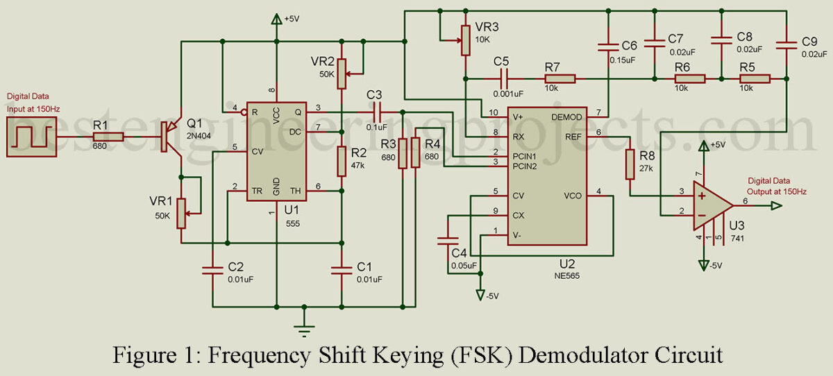
To generate FSK signals, a 555 timer is employed as an astable multivibrator, where the output frequency is determined by the logic state of the digital data input. The standard frequency for data transmission is often set at 150 Hz. When the input is at logic 1, transistor Q1 remains off, allowing the 555 timer to function as an astable multivibrator. In this configuration, capacitor C2 charges through VR1 and R2 until it reaches 2/3 VCC, and then discharges through R2 until it reaches 1/3 VCC as long as the input remains at the logic 1 state. The output waveform frequency can be calculated using the equation:
F0 = 1.45/(RA + 2RB)C = 1070 Hz
By carefully selecting suitable values for VR1, VR2, and R2, a mark frequency of 1070 Hz can be achieved. On the other hand, when the input is at logic 0, transistor Q1 saturates, establishing a connection between resistance VR1 and R2. This connection reduces the capacitor’s charging time, resulting in an increased output frequency. The frequency can be calculated using the equation:
F0 = 1.45/(RA||RC + 2RB)C = 1270 Hz
Through appropriate adjustment of VR1, this frequency is set to match the space frequency of 1270 Hz. The difference between these two FSK signals, namely 1070 Hz and 1270 Hz, is referred to as the frequency shift.
In the configuration depicted in Figure 1, the output of the 555 FSK generator is fed into the 565 FSK demodulator. To eliminate any DC level present, capacitive coupling is employed at the input. Upon the arrival of the signal at the input of the 565 demodulator, the loop efficiently synchronizes with the input frequency, enabling seamless tracking between the two frequencies while simultaneously producing a proportional DC shift at the output. The free-running frequency of the Voltage-Controlled Oscillator is determined by variable resistor VR3 and capacitor C4, while capacitor C6 acts as a loop filter, defining the dynamic characteristics of the demodulator. In order to eliminate overshoot on the output pulse, C6 needs to be chosen to be smaller than usual. A three-stage RC ladder low-pass filter is employed to eliminate the carrier component from the output.
The cutoff frequency (fH = 1/2 ∏RC) of the ladder filter is chosen to be approximately halfway between the maximum keying rate of 150 Hz and twice the input frequency, around 2200 Hz. To ensure compatibility with logic-level requirements, a voltage comparator can be connected between the output of the ladder filter and pin 6 of the PLL, resulting in a logic-compatible output signal of 150 Hz. VR3 is adjusted to set the VCO frequencies in such a way that a slightly positive voltage is obtained at the output when fIN = 1070 Hz.
In conclusion, Frequency Shift Keying (FSK) is a vital technique used in computer peripheral and wireless communication systems for transmitting binary data. By manipulating carrier frequencies, FSK enables efficient and reliable data transfer. The 565 PLL serves as an excellent demodulator for FSK signals, allowing for accurate decoding. Understanding the principles and components of FSK opens up a wide range of applications in modern communication systems.
Component List of Frequency Shift Keying Demodulator Circuit
Resistors (all ¼-watt, ± 5% Carbon)
R1 = 680Ω
R2 = 47 kΩ
R3, R4 = 680 Ω
R5, R6, R7 = 10 kΩ
R8 = 27 kΩ
VR1 = 50 kΩ set at 39.24 kΩ potentiometer
VR2 = 50 kΩ potentiometer
VR3 = 10 kΩ potentiometer
Capacitors
C1, C2 = 0.01 µF
C3 = 0.1 µF
C4 = 0.05 µF
C5 = 0.001 µF
C6 = 0.15 µF
C7, C8, C9 = 0.02 µF
Semiconductors
U1 = NE555 Timer IC
U2 = NE565
U3 = 741 or 351
Q1 = 2N404