This article is intended as a guide to circuit and equipment designers in the operation and application of MOS integrated circuits. It covers general operating and handling considerations with respect to the following critical factors:
- Operating supply-voltage range
- Power dissipation and derating
- System noise considerations
- Power-source rules
- Gate-oxide protection networks
- Input signals and ratings
- Chip assembly and storage
- Device mounting
- Testing
More specific information is then given on significant features, special design and application requirements, and standard ratings and electrical characteristics for COS/MOS A- and B- series logic circuits, and on COS/MOS time-keeping and special circuits.
General Operating and Handling Considerations
The following paragraphs discuss some key operating and handling considerations that must be considered to achieve maximum advantage of the COS/MOS technology.
Operating Supply-Voltage Range
Because logic systems occasionally experience transient conditions on the power-supply line which, when added to the nominal power-bus voltage, could exceed the safe limits of circuits connected to the power bus, the recommended operating supply-voltage ranges are 3 to 18 volts for B-series devices. The recommended maximum power-supply limit is substantially below the minimum primary breakdown limit for the devices to allow for limited power supply transient and regulation limits. For circuits that operate in a linear mode over a portion of the voltage range, such as RC or crystal oscillators, a minimum supply voltage of at least 4 volts is recommended.
Power Dissipation and Derating
The power dissipation of a COS/MOS integrated circuit is the sum of a dc (quiescent) component and an ac (dynamic) component. The dc component is the sum of the net integrated circuit reverse diode-junction current and the surface leakage current times the supply voltage. In standard A- or B-series logic device, the dc dissipation typically ranges, depending upon device complexity, from 100 to 400 milliwatts for a supply voltage of 10 volts. Worst-case dc dissipation is the product of the maximum quiescent current (given in the data sheet on each device) and the dc supply voltage VDD.
The dynamic (ac) power dissipation is approximately equal to the product CV2f, where C is the net output capacitive load being charged and discharged by the integrated circuit, V is the supply voltage, and f is the output switching frequency. The product CV2f account for approximately 90 percent of the dynamic dissipation. The remaining 10 percent is contributed by the momentary flow of IC switching current through the p- and n-MOS transistors to ground.
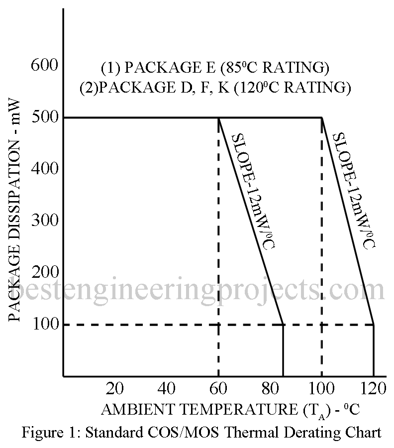
All COS/MOS devices are rated at 200mW per package at the maximum operating ambient temperature rating (TA) for the package type (850C for plastic package and 1250C for ceramic packages). Power rating for temperatures below the maximum operating temperature are shown in the standard COS/MOS thermal derating chart in figure 1. This chart assumes that (a) the device is mounted and soldered (or placed in a socket) on a PC board; (b) there is natural convection cooling, with the PC board mounted horizontally; and (c) the pressure is standard (14.7 psia). In addition to the over-all package dissipation, device dissipation per output transistor is limited 100 mW maximum over the full package operating-temperature range.
System Noise Considerations
In general, COS/MOS device are much less sensitive to noise on power and ground lines than bipolar logic families (such as TTL or DTL). However, this sensitivity varies as a function of the power supply voltage, and more importantly as a function of synchronism between noise spikes and input transitions. Good power distribution in digital systems requires that the power bus have a low dynamic impedance; for this purpose, discrete decoupling capacitors should be distributed across the power bus.
Power Source Rules
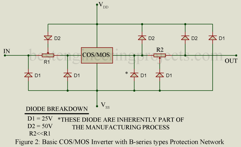
Figure 2 shows the basic COS/MOS inverter and its gate-oxide protection network plus inherent diodes. The safe operating procedures listed below can be understood by reference to this inverter:
- When separate power supplies are used for the COS/MOS device and for the device inputs, the device power supply should always be turn on before the independent input signal sources, and the input signals should be turned off before the power supply is turned off (
as a maximum limit). This rule will prevent over dissipation and possible damage to the D2 input-protection diode when the device power supply is grounded. When the device power supply is an open circuit, violation of this rule can result in undesired circuit operation although device damage should not result; ac inputs can be rectified by diode D2 to act as a power supply.
- The power supply operating voltage should be kept safely below the absolute maximum supply rating, as indicated previously.
- The power supply polarity for COS/MOS circuits should not be reversed. The positive (VDD) terminal should never be more than 0.5-volt negative with respect to the native (VSS) terminal (VDD-VSS > -0.5V). Reversal of polarities will forward-bias and short the structural and protection diode between VDD and VSS.
- VDD should be equal to or greater than VCC for COS/MOS buffers which have two power supplies (in particular, for CD4009 and CD4010 COS/MOS-to-TTL “down”-conversion devices).
- Power-source current capability should be limited to as low a value as reasonable to assure good logic operation.
- Large value of resistors in series with VDD or VSS should be avoided; transient turn-on of input protection diodes can result from drops across such resistors during switching.
Gate-Oxide Protection Network
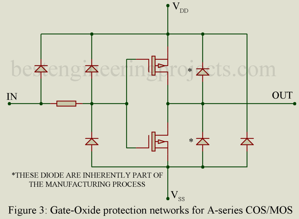
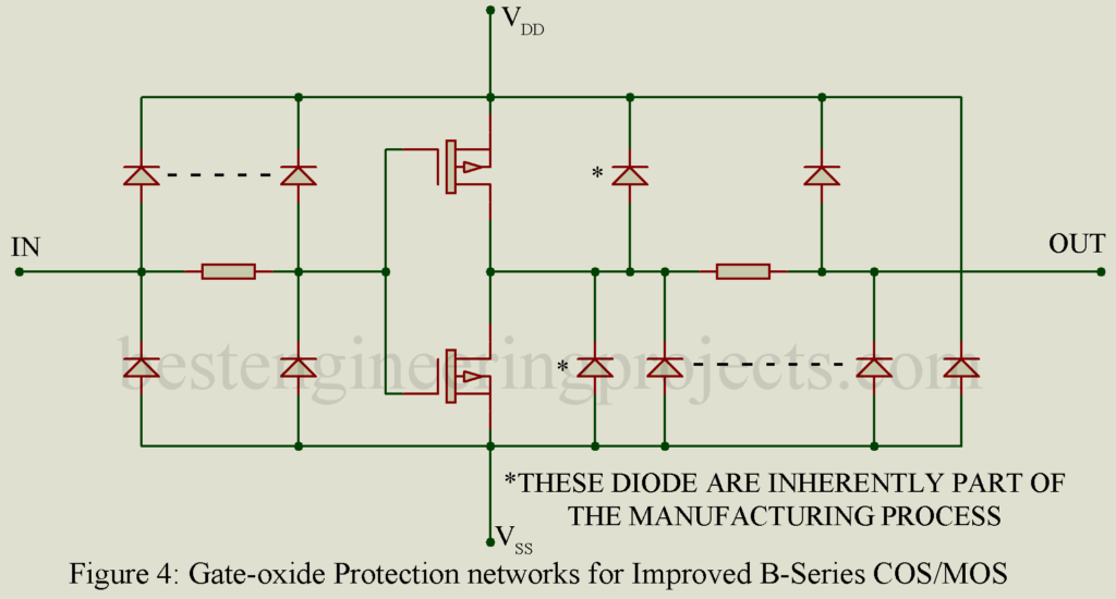
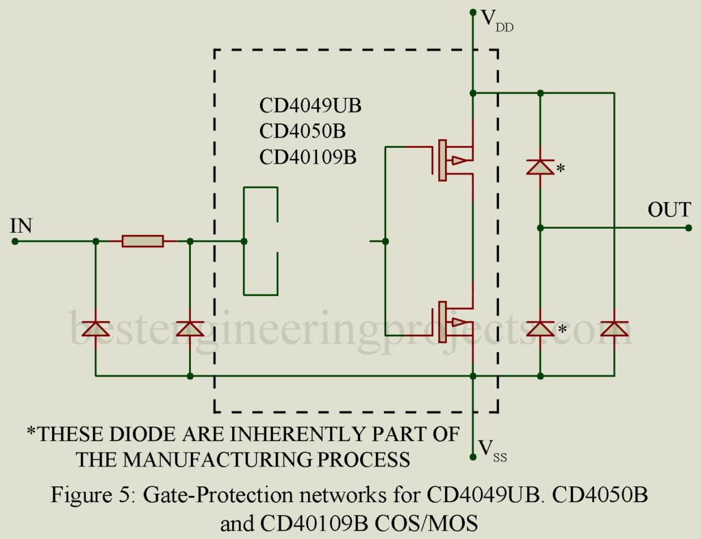
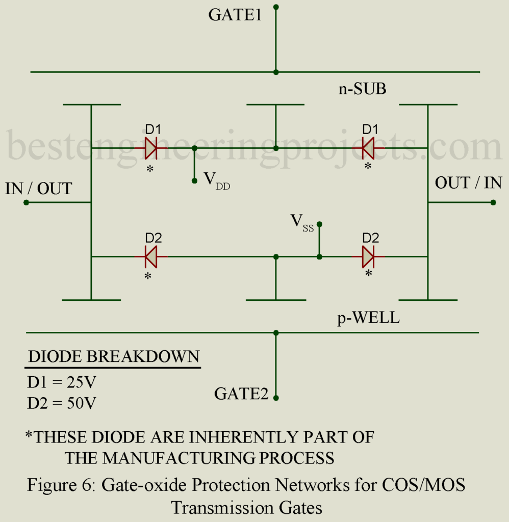
A problem occasionally encountered in handling and testing low-power semiconductor devices, including MOS and small-geometry bipolar devices, has been damage to gate oxide and/ or p-n junction. Figure 3, 4, 5, and 6 shows the gate-oxides protection circuits used to protect COS/MOS devices from static electricity damage.
Input Signals and Ratings
- Input signals should be maintained within the power-supply voltage range,
. In applications such as astable and monostable multivibrators, input current can flow and, for optimal performance, should be limited to 100 microamperes by use of a resistor in series with the input terminal. The added protection assures proper circuit operation and prevents possible parasitic bipolar effects.
- All COS/MOS inputs should be terminated. When COS/MOS inputs are wired to edge card connectors with COS/MOS drive coming from another PC board, a shunt resistor should be connected to VDD or VSS in case the inputs become unterminated with the power supply on.
- When COS/MOS circuits are driven by TTL logic, a “pull-up” resistor should be connected from the COS/MOS input to 5 volts.
- Input signals, should be maintained within the recommended input-signal-swing range.
Output Rules
- The power dissipation in a COS/MOS package should not exceed the rated value for the ambient temperature specified. The actual dissipation should be calculated when (a) shorting outputs directly to VDD or VSS, (b) driving low impedance loads, or (c) directly driving the base of p-n-p or n-p-n bipolar transistor.
- Output short circuits often result form testing errors or improper board assembly. Shorts on buffer outputs or across power supplies greater than 5 volts can damage COS/MOS devices.
- COS/MOS, like active pull-up TTL, cannot be connected in the “wire-OR” configuration because an “on” PMOS and an “on” NMOS transistor could be directly shorted across the power-supply rails.
- Paralleling inputs and outputs of gates is recommended only when the gates are within the same IC package.
- Output loads should return to a voltage within the supply-voltage range (VDD to VSS).
- Large capacitive loads (greater than 5000 pF) on COS/MOS buffers or high-current drivers act like short circuits and may over-dissipate output transistors.
- Output transistors may be over dissipated by operating buffers as linear amplifiers or using these types as one-shot or stable multivibrators.
Noise Immunity and Noise Margin
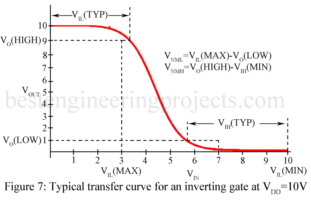
The complementary structures of the inverter, common to all COS/MOS logic devices, results in a near-ideal input-output transfer characteristic, with switching point midway (45% to 55%) between the 0 and 1 output logic levels. The result is high dc noise immunity.
Figure 7 shows a typical transfer curve that may be used to define the noise immunity of COS/MOS integrated circuits. The noise-immunity voltage (VIL or VIH) is the noise voltage at any one input that does not propagate through the system. Minimum noise immunity for buffered B-series COS/MOS devices is 30, 30 and 27 percent, respectively for supply voltage VDD of 5, 10 and 15 volts and 20 percent of VDD for all unbuffered gates. The VIL and VIH specifications define the maximum permissible additive noise voltage at an input terminal when input signals are within 50 millivolts of the supply rails.
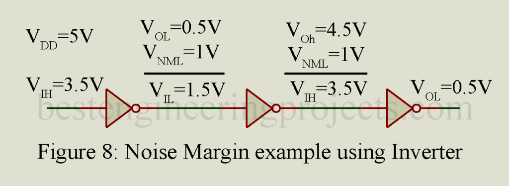
Noise margin is the difference between the noise-immunity voltage (VIL or VIH) and the output voltage Vo. Noise margin voltage is the maximum voltage that can be impressed upon an input voltage VIN (where VIN is the VOL or VOH voltage of the preceding state) at any (or all) logic I/O terminals without upsetting the logic or causing any output to exceed the output voltage (VO) conditions specified for VIL and VIH rating. Figure 8 illustrates the noise margin concept in a simple system. Noise margin for buffered B-series COS/MOS devices are 1, 2, and 2.5 volts, respectively, for supply voltages of 5, 10 and 15 volts.
Of the two noise-limitation specifications (noise immunity and noise margin), RCA considers noise immunity to be more practical for COS/MOS devices because COS/MOS outputs are normally within 50 millivolts of supply rails.
Noise immunity increases as the input pulse width becomes less than the propagation delay of the circuit. This condition is often described as ac noise immunity.
Clock Rise-and Fall-Time Requirements
Most COS/MOS clocked devices have maximum rise-and fall-time ratings (normally 5 to 15 microseconds). With longer rise or fall times, a device may not function properly because of data ripple-through, false triggering problems, etc. Whenever feasible, B-Series COS/MOS counters have Schmitt trigger shaping circuits built into the clock circuit thereby negating the restriction for input rise or fall times of 5 to 15 microseconds. Long rise and fall times on COS/MOS buffer-type inputs causes increased power dissipation which may exceed device capability for operating power supply voltages greater than 5 volts.
Parallel Clocking
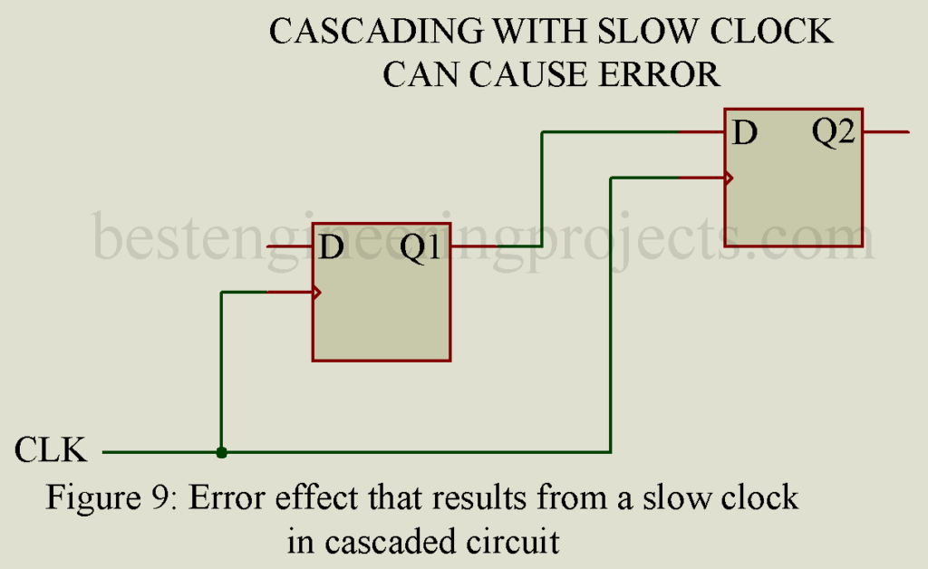
Process variations leading to difference in input threshold voltage among random device samples can cause loss of data between certain synchronously clocked sequential circuits, as shown in figure 9. This problem can be avoided if the clock rise time (txCL) is made less than the total of the fixed proportion delay plus the output transition time of the first stage, as determined from the device data for the specific loading condition in effect. Schmitt trigger circuits such as the CD4093B are an ideal solution to applications required wave shaping.
Three-State Logic
Three state logic can be easily implemented by use of a transmission gate in the output circuits; this technique provides a solution to the wire-OR problem in many cases.
Chip Assembly and Storage
RCA COS/MOS integrated circuits are provided in chip form (H suffix) to allow customer design of special and complex circuits to suit individual needs. COS/MOS chips are electrically identical and offer the features of their counterparts sealed in ceramic and plastic packages. The following paragraphs describe mounting considerations, packaging, shipping and storage criteria, handling criteria, visual inspection criteria, testing criteria, and bounding pad layout and dimensions for each chip.
Mounting Considerations. All COS/MOS chips are non-gold blacked and require the use of epoxy mounting. DuPoint NO. 5504A conductive silver paste or equivalent is recommended. In any case the manufacturer’s recommendations for storage and use should be followed. If DuPoint NO 5504 paste is used, the bond should be cured at temperatures between 1850C an d 2000C for 75 minutes.
In COS/MOS circuits MOS-transistor p-channel substrate (n-type bulk material) are connected to VDD, therefore, when chips are mounted and a conductive paste is used care must be taken to keep the active substrate isolated from ground or other circuit elements.
Packing, Shipping, and storage criteria. Solid-state chips, unlike packaged device, are non-hermetic devices, normally fragile and small in physical size, and therefore, require special handling considerations as follows:
- Chip must be stored under proper conditions to ensure that they are not subjected to a moist and/or contaminated atmosphere that could alter their electrical, physical, or mechanical characteristics. After the shipping container is opened, the chip must be stored under the following conditions:
- Storage temperature, 400C max.
- Relative humidity, 50% max.
- Clean, dust-free environment
- The user must excursive proper care when handling chips to prevent ever the slightest physical damage to the chip.
- During mounting and lead bonding of chips the user must use proper assembly techniques to obtain proper electrical, thermal, and mechanical performance.
- After the chip has been mounted and bonded, any necessary procedure must be followed by the user to ensure that these non-hermetic chips are not subjected to moist and contaminated atmosphere which might cause the development of electrically conductive paths across the relatively small insulating surface. In addition, proper consideration must be given to the protection of these devices from other harmful environments which could conceivably adversely affect their proper performances.
Handling Criteria.
The user should find the following suggested precautions helpful in handling COS/MOS chips.
In any event, because of the extremely small size and fragile nature of chips, the equipment designer should exercise care in handling these devices.
- Grounded
- Bonders, pellet pick-up tools, table tops, trim and form tools, sealing equipment, and other equipment used in chip handling should be properly grounded.
- The operator should be properly grounded.
- In-process handling
- Assemblies or subassemblies of chips should be transported and stored in conductive carriers.
- All external leads of the assemblies or subassemblies should be shorted together.
- Bonding Sequence
- Connect VDD first to external connections, for example, terminal 14 of the CD4001AH.
- Remaining function may be connected to their external connections in any sequence.
- Testing
- Transport all assemblies of chips in conductive carriers,
- In testing chip assemblies or subassemblies, the operator should be properly grounded.
Visual Inspection Criteria
All standard commercial COS/MOS chips undergo a visual inspection which is patterned after MIL-STD-883, Method 2010.1. Conduction B with modifications reflecting COS/MOS requirements.
Testing Criteria. COS/MOS chips are dc electrically tested 100% in accordance with the same standards prescribed for RCA devices in standard packages.
Device Testing
RCA COS/MOS circuits are 100-percent tested by circuit probe in the wafer stage and are 100-percent tested again after have been packaged. DC tests of RCA devices are performed at 5, 10, 15 and 20 volts; functionality is checked at 3, 17, and 22 volts depending family (i.e., A and B series). Sample testing is used to assure adherence to quality requirements and ac specifications.
Static tests, high-speed functional and dc parametric tests, are performed at wafer and package stages by means of a Teradyne J283 test set. A Teradyne S157CM test set and a Marcodata MD154 test set are used in dynamic testing. Dynamic testes are performed with 15 and 50 picofarad loads. Testing at 15 picofarad is accomplished primarily by laboratory “bench-test” techniques; automatic testing at 15 picofarads is difficult because of the high input capacitance (approximately 20 to 35 picofarads) of most automatic ac test sets.
Users should follow the sequence below when testing COS/MOS devices:
- Inserts the device into the test socket
- Apply VDD
- Apply the input signal
- Perform the test
- On completing of test, remove the input signal
- Turn off the power supply (VDD)
- Remove the device from the test socket and insert it into a conductive carrier. COS/MOS devices under test must not be exposed to electrostatic discharge or forward biasing of the intrinsic protective diodes shown in figures 3, 4, 5, and 6.
