The project phase sequence change indicator using 555 IC is used to indicate whether there is a change in phase sequence occurring or not by a beeper or a LED. We all know that in three-phase motor phase sequence is important because the change in phase sequence may cause trouble in machines.
Circuit Description of Phase Sequence Change Indicator
The circuit of phase sequence change indicator is divided into two main sections i.e. controlling section and the beeper section. The circuit of the phase sequence change indicator is shown in figure 1.
The three transistors T1, T2, and T3 are used to change three-phase waveforms into square waveforms. The resistor is connected to its base and is so selected that the transistor gets fully saturated when the base voltage becomes 10V. The diode connected to its base keeps the reverse voltage below 0.6V during the negative cycle.
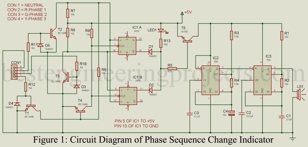
When the phase sequence is correct, the red phase lags the yellow phase by 1200 whereas the green phase lags the red phase by 1200. The circuit is designed here to detect any change in the sequence as above and further procedure beeping sound. Phase inversion and decrement of the slope of rising and falling edge (i.e. to decrement the rise time of the square wave) is done by transistor T4. The output of transistor T4 is connected to the clock pin (pin 6 and pin 1) of IC7476 (IC1) as a result during every cycle the phase sequence is checked.
For the clock, the squared waveform of the yellow phase is used. Other phases are inverted during squaring operation. So, at the falling edge, transistor T3 is cut-off and T2 is in saturation. The Collector of T2 is connected to the input J of IC1:a and K of IC1:b. So at the clock edge, we got low at both the inputs. Collectors of T3 are connected to K input of IC1:a and J of IC1:b resulting in high output at the clock pulse. At the rising edge of the clock, we get J low and K high for IC1:a. So it gets reset and gives high at Q. Similarly when the J and K inputs of IC1:b are high the flip-flop is set. The Q output of IC1:a and Q output of IC1:b are ORed and fed at the base of T5 to switch on the beeper circuit. The beeper circuit is designed using two timer IC 555 and both are configured in astable multivibrator mode.
Check out other interesting projects posted on bestengineeringprojects.com
- Single Phase Preventer with Under/Over Voltage Cutout
- 3 Phase Induction Motor Starter
- Motor Controller Circuit for Washing Machine
PARTS LIST OF PHASE SEQUENCE CHANGE INDICTOR
| Resistors (all ¼-watt, ± 5% Carbon) |
| R1, R2 = 22 KΩ
R3, R4 = 5.6 KΩ R5 = 470 Ω R6 – R9 = 10 KΩ R10 – R12 = 1 MΩ R13 = 560 Ω |
| Capacitors |
| C1, C3 = 0.1 µF (Ceramic Disc)
C2 = 0.01 µF (Ceramic Disc) C4 = 10 µF/16V (Electrolytic Capacitor) |
| Semiconductors |
| IC1 = 7476 (Dual J-K Flip-Flip IC)
IC2, IC3 = NE555 (Timer IC) T1 – T4 = BC148B (silicon NPN epitaxial planar transistor) T5 = SK100 (general purpose, medium power PNP transistor) D1 – D4 = 1N4001 (Rectifier Diode) LED1 = 5mm Any Color LED |
| Miscellaneous |
| LS1 = 8Ω Speaker |