What is Open Circuit PN Diode?
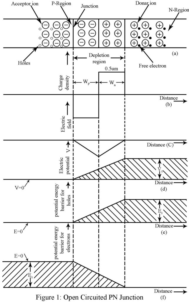
Figure 1(a) shows an open circuited pn diode with acceptor impurity density NA in the p-region and donor impurity density ND in the n-region. We assume that each acceptor atom has ionized resulting in one immobile negatively charged acceptor ion and one mobile hole. Similarly, each donor atom has ionized resulting in one immobile positively charged donor ion and one mobile electron. In Figure 1(a) the immobile acceptor ion is indicated by a minus sign enclosed within a circle while immobile donor ion is indicated by a plus sign enclosed within a circle. We assume that in the beginning there are only holes in the p-region (on the left of the junction) and only electrons in the n-region (on the right hand of the junction).
Space Charge region or Depletion Region | Open Circuit PN Diode
In the beginning there exists a density gradient of holes across the junction from left to right and density gradient of free electrons from right to left. Hence, holes diffuse across the junction from p-region to n-region while free electron diffuse across the junction from n-region to p-region. The hole on entering the n-region combine with electrons in the vicinity of the junction. These electrons which originally covered or neutralized the positive donor ions near the junction are thus lost through combination with the incoming holes. This process leaves the positive ions unnaturalized or uncovered. Similarly, negative electrons on diffusing across the junction into the p-region combine with holes in the vicinity of the junction. These, holes which initially neutralized or covered the negative ions are thus lost through recombination. This process leaves the negative ions unnaturalized or uncovered. Figure 1(b) gives the typical shape of the charge density plotted against distance. The exact shape of this curve depends on the diode junction whether uniform graded or step graded or step graded or any other type.
The region of the junction has been depleted of mobile charge carriers. Hence, this region is referred to as the depletion region. It is also called space charge region or the transition region. The depletion region is extremely thin, typically 0.5 micron (0.5×10⁻⁶m) thick. To the left of the depletion region, the mobile carrier density is while to the right, the carrier density is
.
Electricity Field Intensity | Open Circuit PN Diode
From figure 1(b) we find that the space charge density is zero at the junction, positive to the right and negative to the left. Such a charge distribution forms an electric poles and results in electric lines of flux from right to left. This corresponding electric filed intensity is negative and varies with distance in the transition region as shown in figure 1(c). This electric filed tends to send a drift current from right to left opposing the diffusion current. Accordingly, as the diffusion of carriers across the junction progresses, depletion of mobile carriers progresses, electric field builds up until an equilibrium, is reached when the electric field completely disallows the process of diffusion of charge carriers. Under the steady state, hole (electron) diffusion current resulting in net zero-hole (electron) current, an essential condition in an open circuited device.
Poisson’s equation states, (1)
Where is the electrical permittivity?
Then the electric field is given by,
…….(2)
Where at X = X0, Where X0 represents the left edge of the depletion region.
Potential V | Open Circuit PN Diode
The electrostatic potential V is given by,
(3)
Thus, the electrostatic potential V is the negative of the integral of the electric field of figure 1(c). Figure 1(d) plots the electrostatic potential V against distance x in the depletion region taking the potential of the p-region as the reference potential or zero potential. Then, the potential of the n-region is higher by V0 as shown in figure 1(d). The potential difference V0 built across the junction is nothing but the contact potential V0 as is given by
…….(4)
Value of V0 is from 0.2 to 0.4 volts for Ge and from 0.5 to 0.9 volt for Si. This V0 is considerably larger than the average thermal energy 0.02eV for the charge carriers at T=300 K.
Potential Energy Barrier | Open Circuit PN Diode
The potential energy E equals the product of potential V and the charge of the carrier. Thus, Figure 1(e) plots the potential energy barrier against further diffusion of holes from the p-region to n-region taking E = 0 in the p-region. The height of the potential energy barrier in joules equals E0 = qV0 is in volts. Similarly, the potential energy barrier against the flow of electrons from n-region to p-region equals -qV0 and is plotted in Figure 1(f) taking E = 0 in the p-region.
Example 1:
- The resistivities of the p-region and the n-region of a Ge pn diode are 5-ohm-cm and 3-ohm-cm respectively. Calculate the height of the potential energy barrier.
- Repeat part “a” if the doping density of p and n regions each are doubled. Given that: Q 1.6 X 10⁻¹⁹ columb;
cm2/V-s,
cm2/V-s, volt-equivalent of temperature at 300 K is 0.026 volt and ni = 2.5×10¹³/cm3.
Solution:
For (a)
Hence, /cm3
Similarly, /cm3
Hence,
Hence,
For (b)
Hence,
