In the article Flip flop IC, we will discuss about key parameter of flip flop IC, its working, truth table application and comments.
Description of Flip Flip IC
One of the key building blocks of all digital logic systems, the flip-flop (FF) is available in a variety of different FF circuits with a host of different features.
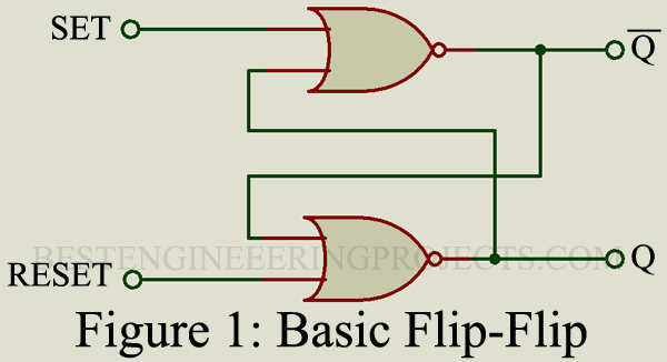
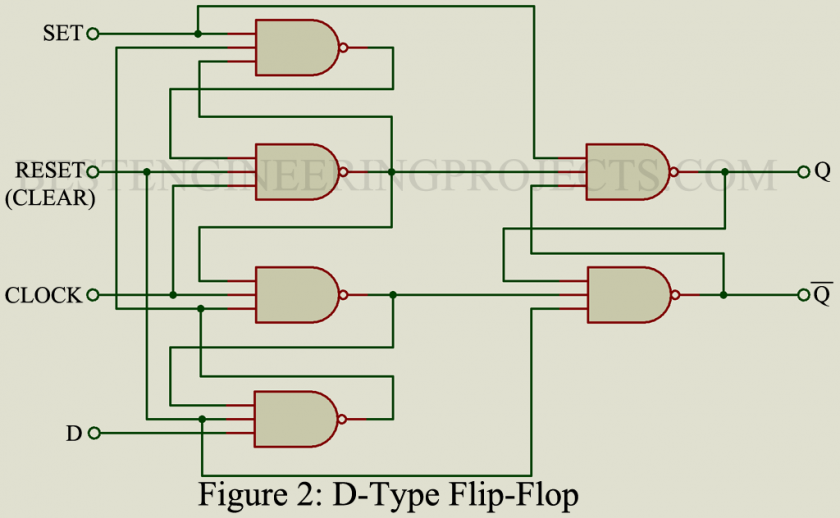
As illustrated in Figure 1, the basic flip-flop consists of two gates with the appropriate cross connection. The actual circuitry of a D-type, positive edge triggered FF is shown in figure 2, and illustrates the application of different gating circuits to the basic FF function. Note the presence of the “clock,” “reset” (clear), and “set” inputs in addition to the actual data input, terminal D. The logic level at input D is transferred to the Q output only during the positive going edge of the clock pulse. When the clock pulse is at either the 0 or the 1 level, the D input signal has no effect. The “set” input signal can set the condition of the FF anytime, regardless of the presence or absence of a clock pulse. Similarly, the “reset” signal can restore the condition of the FF any time.
The detailed operation of the FF is summarized by the truth table of figure 3. The set and reset (clear) operations can occur regardless of the presence of the clock pulse, but data inputs at terminal D can occur only during the positive edge of the clock pulse when the set and reset signals are 0. If both set and clear signals are 1, simultaneously, it is possible for both Q and signals to be 1 at the same time. The actual condition of the output is undermined and unpredictable in this situation.
Truth Table of Flip Flip IC
| Clock | Data | Reset | Set | Q | Q |
| 1 | 0 | 0 | 0 | 0 | 1 |
| 1 | 1 | 0 | 0 | 1 | 0 |
| 1 | X | 0 | 0 | NC | NC |
| X | X | 1 | 0 | 0 | 1 |
| X | X | 0 | 1 | 1 | 0 |
| X | X | 1 | 1 | 1 | 1 |
Key Parameters
- Maximum power dissipation: The maximum power that the IC can dissipate over the specified temperature range, usually from -400 to +850
- Quiescent current: The current drawn when the FFs on the entire IC are not operating.
- Toggle rate: The maximum frequency at which the FF can change state.
- Propagation delay, clock to output: The time required from the clock pulse transition until a change takes place in the FF output terminal.
- Propagation delay, set or reset to output: The time delay from the application of the set or reset signal until the output state changes.
- Clock pulse width: The minimum width of the clock pulse required for reliable operation.
- Set or reset pulse width: The minimum width of the set or reset pulse.
Applications
FFs of every type are found in IC applications such as counters, shift registers, microprocessors, memories, etc. ICs containing a small number of FFs on which all terminals are available are used as auxiliary circuits in digital systems. FFs are used as short-time delays, set-reset switches, and in a host of other control applications.
Comments
FFs are available in every digital logic IC family and can be obtained in a wide variety of characteristics and operational features.

