A single beam CRO can be used for simultaneous display of two signals using this simple circuit “Dual Trace Generator Circuit”. The circuit uses one NE555 and two LM741 ICs, besides some passive components. The diode (1N4148) is used to get a 50 percent duty cycle.
Circuit Description of Dual Trace Generator Circuit
IC 555 is connected in astable mode and acts as a self-switching analog switch between the two signals to be displayed on the CRO. The output of IC 555 is given to the CRO. In order to display the two waveforms at different positions, a DC shift is given to one of the waveforms.
The output of IC2 switches between two voltage levels (Vcc and GND) at pin 8 and 1. The frequency of switching is decided by the external RC network. The output frequency of IC 555 is independent of the supply voltage and remains constant over the entire operating range of voltage, i.e. from 3V to 18V. Therefore, if two independent time-varying signals are fed at pins 1 and 8, the output of IC3 will switch between the voltage levels at two pins with constant frequency. The signals should be within the operation range and of correct polarity.
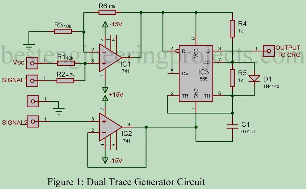
One of the signals to be displayed is given sufficient positive DC shift and fed at the Vcc terminal. The other signal is fed at the ground terminals (pin 1) of IC 555 through a buffer. The output of IC555 automatically switches between these two levels and the signals are displayed on the CRO with the given DC shift between these levels. The tracing between these levels is not visible because the switching frequency is very high compared to the frequency of input signals.
Each 741 is connected as a unity-gain adder in the non-inverting mode, to give the required DC shift to one of the waveforms. When there is on signal, two beams will be displayed on the CRO.
Since it is a measuring instrument, the circuit will not load the source, i.e. minimum current will be drawn from the source.
The DC shift should be sufficient for the worst conditions of input signals, i.e. when signal 2 is at its positive peak and signal 1 is at a negative peak, the potential difference between these terminals should not be less than 5V. when signal 1 is at a positive peak and signals 2 at a negative peak, the potential difference should not exceed 18V.
The capacitors of 0.01 µF, normally connected between pins 1 and 5, are not connected to avoid unwanted modulation of the displayed waveforms. For large waveforms, the input signals must be attenuated before feeding the circuit.
One disadvantage of the circuit is that the signals cannot be overlapped on the CRO for comparison.
PARTS LIST OF DUAL TRACE GENERATOR CIRCUIT
| ResiNostor (all ¼-watt, ± 5% Carbon) |
| R1, R3, R6 = 10 KΩ
R2 = 4.7 KΩ R4, R5 = 1 KΩ |
| Capacitor |
| C1 = 0.01 µF (Ceramic Disc) |
| Semiconductor |
| IC1, IC2 = LM741 (General purpose operational amplifier)
IC2 = NE555 (Timer IC) D1 = 1N4148 (standard silicon switching signal diode) |
Note: The circuit uses neutral as the reference line for waveform generation. There is no provision in the circuit for indicating a phase failure. Supply voltage to the circuit is 5 volts, and phase checking inputs are connected directly to the phase through a voltage divider.