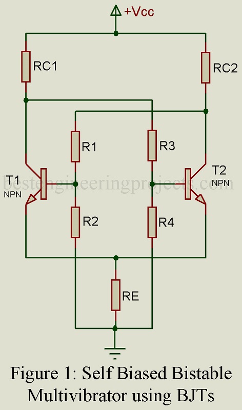
Bistable Multivibrator generates a square wave but has two stable states. The circuit stays in one stable say state one indefinitely. Only on application of a suitable trigger pulse, circuit changes to the other stable state i.e. state two. Now again the circuit continues to stay in stable state two indefinitely unless a suitable trigger pulse is applied causing the circuit to revert to the stable state one.
Bistable multivibrators are basically of two types:
(i) Fixed bias bistable multivibrator
(ii) Self bias bistable multivibrator
We here take up the study of a simple self-biased stable multivibrator
Self-Bias Bistable Multivibrator using BJTs
Figure 1 gives the basic circuit using a common resistor R1 from emitter to ground. It is also referred to as Eccles-Jordon bistable multivibrator. The voltage drop across Ri provides the self-bias for keeping one of the transistors in the OFF state.
Operation of the Bistable Multivibrator Circuit
Since T1 is nonconducting the base current of T2 is . If R3 is small enough, this base current is large enough to saturate T2. Then the saturation voltage of T2 is smaller than the turn-on voltage of T1. Thus, essentially no base current flows through R1 and T1 is cutoff as assumed earlier. The multivibrator remains in this stable state until a suitable switching pulse is applied at some point in the circuit to turn T1 ON. Then T1 will saturate and its saturation voltage will be insufficient to provide forward bias to T2 with the result that T2 will be turned OFF.
The multivibrator will remain in this second state until another suitable switching pulse is applied at a suitable point in the circuit to turn T2 ON and T1 OFF. Thus, this multivibrator has two stable states and is, therefore, called bistable multivibrator. It is also known as slip-flop because a trigger pulse will make it flip or flop from one state to the other. The trigger pulse is needed only to start conduction of the OFF transistor and the circuit regeneration or positive feedback will carry out the change of state.
This may be seen from figure 2. Thus, if T1 begins to conduct, its collector voltage decreases and T2 is pulled out of saturation. The collector voltage of T2 then rises and forward bias is applied through R1 to reinforce the initial trigger. This effect is cumulative and the change of state is completed. It may be noted that the change of state can be initiated with a very small pulse if T2 is just barely saturated. However, if T2 is heavily saturated then the trigger pulse must be large in magnitude and must remain long enough to permit T1 to pull T2 out of saturation.
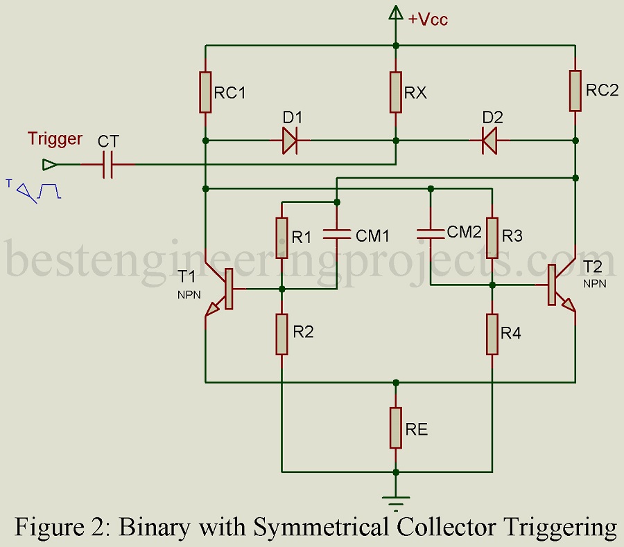
Bistable Multivibrator with Symmetrical Collector Triggering:
Fig. 2 gives the circuit of binary (flip-flop) using symmetrical collector triggering where trigger tries to turn OFF a Saturated or ON transistor. The negative trigger is applied through coupling capacitor CT to point P which is connected to VCC through resistor RX. The RX-CT network forms the differentiating circuit. The input pulses after differentiation appear at point P to which cathodes of two steering diodes D1 and D2 are connected. Anodes of the diodes D1 and D2 are connected to the collectors of the transistors T1 and T2 respectively.
Diodes serve to permit binary to respond to only one polarity of pulse. Thus, with transistor T1 ON, diode D1 is reverse biased by an amount equal to the Voltage drop across Rc1. Diode D1 then does not transmit any triggering signal unless the signal is negative and has amplitude exceeding the voltage drop across Rc1. However, with T1 OFF, voltage drop across diode D1 is zero. But the diode still does not transmit a positive trigger signal but does transmit a negative step or pulse to the input of ON transistor T2. However, resistor RX must be sufficiently large So as not to load the trigger source.
With transistor T1 OFF, there is no collector current and hence Zero Voltage drop across resistor Rc1. The collector voltage of T1 then equals the supply Voltage VCC. The anode and the cathode of diode D1 are at the same potential namely VCC. Diode D1 is forward biased. The voltage drops across the collector circuit resistor Rc2 of conducting transistor T2 makes the collector voltage of T2 very low equal to Vc2, ON. Thus, anode of diode D2 is at a low potential while the cathode is at VCC. Hence diode D2 is reverse biased.
The differentiated pulse appears at point P. Polarities of steering diodes are such that they block the transmission of positive pulses. Only the negative pulses follow the low impedance path offered by diode D1 and Coupling network R3-cm2 to the basic of ON transistor T2. This negative pulse assisted by the regenerative feedback of binary pulls the transistor T2 from saturation to OFF state and simultaneously bring T1 into saturation.
Now diode D1 is reverse biased while D2 is forwarded biased. Next negative trigger gets transmitted through D2 and appears at the collector of OFF transistor T2. This negative trigger pulse passes through the coupling network R1-cm1 and appears at the base of the ON transistor T1 and turns it OFF.

