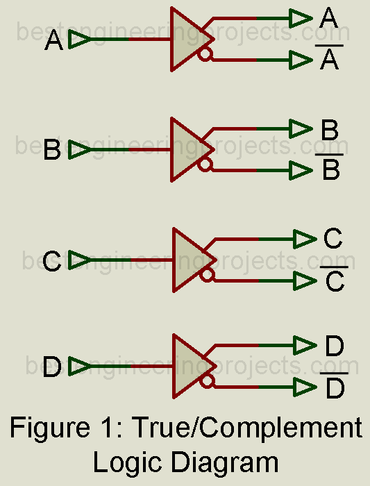
In the article “True Complement Buffer IC | CD4041” we will discuss about true complement buffer IC, it’s key parameters and application.
Description of True Complement Buffer IC | CD4041
Usually available with four identical circuits on a single IC, this buffer provides both the true output and its complement. As illustrated in figure 1, the complement of the input is provided by a single inverter stage while the true output is provided by two stages. The circle at the input of the second stage indicates that, while this circuit is an inverter, its output will be the true or original signal and not the inverted one.
In all other respects the buffer inverter circuit of figure 1 are the same as the standard buffer inverter described in previous article Buffer or inverter IC.
Key Parameters
The electrical characteristics are the same as those for the particular digital IC family.
- Quiescent Current: The total current drawn by the IC when it is not operating. 0.02 uA is typical for high-voltage CMOS devices at power supply voltages up to 15 V.
- Propagation delay time: The time required for the input signal to reach the output. In a true complement buffer, it is important that the propagation delay for both outputs be exactly the same. 60 ns is a typical value for high voltage CMOS devices.
Applications
These buffers are particularly useful for MOS clock drivers, providing both clock phases. They are also used to drive ladder or “weighted R” resistor networks, transmission lines, and digital displays. The fact that both the true and the complement of the input is available makes this IC vary versatile in digital data link equipment.
