Here in this article we will discuss about Non-Inverting 3 State Buffer, its key parameters and its applications.
Non-Inverting 3 State Buffer Description:
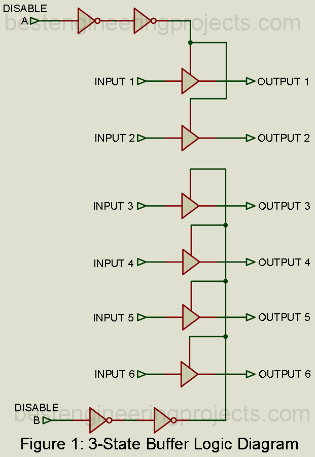
This IC contains six identical non-inverting buffers, arranged in two groups, as illustrated in figure 1. The first group of two buffers is controlled by the “disable A” signal. The seconds group of four buffers is controlled by the “disabled B” signal. This provides three possible output states. When the respective disable signal is 0, the output will be the same as the input, with the usual buffer effect. When either disable signal is 1, the buffers it controls will be turned off and, regardless of input signal, the output will represent a high impedance.
Key Parameters
The electrical characteristics will be the same as for the particular digital IC family.
- Turn-on delay time: The time required from the input of either A or B disable signal until the respective outputs reach the high impedance state. 75 ns is typical for low power CMOS device at 5V power supply.
- Tun-of delay time: The required after either the A or B disable signal has disappeared until the outputs return to their normal state. 75 ns is a typical value for low power CMOS devices at 5V power supply voltage.
- 3-state propagation delay time: The time required from input to output signal at differential conditional. Typical low power CMOS values are:
1 to high impedance: 75 ns.
0 to high impedance: 80 ns.
High impedance to 1: 65 ns.
High impedance to 0: 100 ns.
Applications
Three state buffers are frequently used at the input output ports or bus interfaces of computers and other digital devices. This type of IC is found wherever the flow of parallel digital data s controlled.
Representative Part Number: Texas Instruments SN74126
Comments
If the disable A and disable B signals are combined, all six buffers can be controlled by a single signal. The particular arrangement of two and four permits the user to provide separate disable signal for control and data signals on a typical digital data bus.