Various remote control-based projects are already posted on bestengineeringprojects.com. Now here is a unique remote control circuit called a sound operated on-off switch and it responds only particular frequency of sound (4.5 kHz) and can control the device from a distance of up to 4.6 meters (15 feet).
Most sound-operated switches use clap sound or voice to activate the remote control. Tone frequency generated by clapping or a voice control is not constant and designing a receiver circuit for a particular or ordinary clap or voice is very difficult. To overcome this problem we designed and verified a unique circuit called a sound-operated on-off switch. The unique about this circuit is, it works only on a particular tone frequency.
Circuit Description of Sound Operated On-Off Switch:
As all remote control circuit utilizes two main sections i.e. transmitter unit and the receiver unit.
Transmitter unit | Sound Operated On-Off Switch
The block diagram of the transmitter unit (sound generator) is shown in figure 1. It contains a tone generator, speaker driver, and speaker.

The heart of the circuit for transmitter units is a phase-locked loop (PLL) tone decoder (IC1). IC1 contains VCO (Voltage controlled oscillator) and is used to generate a frequency of 4.5 kHz signal. The output tone frequency is given to the base of speaker driver transistor T1 which further drives the loudspeaker.

Receiver Circuit | Sound Operated On-Off Switch
The Block diagram of the receiver circuit is given in figure 3. This unit is further divided into four subunits i.e. tone amplifier, PLL tone decoder, flip-flop section, and relay driver unit.

Tone amplifier | Sound Operated On-Off Switch
In the circuit, sound operated On-Off switch microphone is used as a sensor. Mic1 receives a tone signal of 4.6 kHz from a tone generation or transmitter circuit and converts it into an electric signal. The output electric signal from the microphone is very weak and need amplification, which is done by transistor T1 and T2. Transistors T1 and T2 are configured as two-state, high gain AF pre-amplifier.

PLL tone decoder | Sound Operated On-Off Switch
We use LM567 in both encoder and decoder units to obtain identical wave-shapes of the signal. The amplified output from transistor T2 is given to the PLL tone decoder (IC2), which is tuned for a center frequency of 4.5 kHz. As a result, the output of IC2 goes low.
Flip-flop section | Sound Operated On-Off Switch
The high-to-low pulse from the PLL tone decoder is given to the clock input pin 13 of the dual JK flip-flop wired around CMOS IC CD4027 (IC3). One of the two flip-flops inside IC3 acts as a square-wave shaper. The square-wave pulse generated by this flip-flop is coupled to the second flip-flop of the IC. This eliminates the need for an extra monostable multivibrator IC.
Relay driver | Sound Operated On-Off Switch
The output of the flip-flop section (IC3) is given to the base of transistor T1 through resistor R16 for amplification. The amplified output from the emitter is given to the base of relay driver transistor T2, which drives the load connected to N/O contacts of the relay as shown in Fig. 4.
Check out other sound operated circuits posted in bestengineeringprojects.com
- Sound Operated Intruder Alarm with Flash
- Sound Operated Relay Using Transistors
- Sound Operated Light and Alarm Circuit
- Op-Amp 741 Based Sound Operated Light
Power supply | Sound Operated On-Off Switch
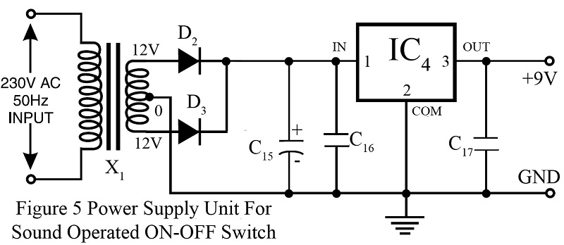
Fig. 5 shows the power supply circuit for the receiver unit. The mains AC supply of 230V is stepped down by 12V-0-12V transformer X1. The output of the secondary transformer is rectified by a full-wave rectifier comprising diodes D1 and D2 and filtered by capacitor C15. The filtered output is given to the input pin of the voltage regulator IC (IC4). The regulated 9V is obtained at the output (pin 3) of IC4 powers the entire receiver circuit.
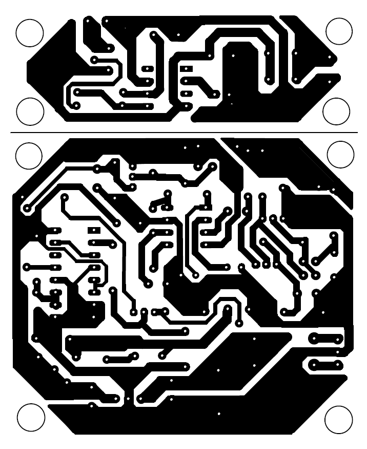
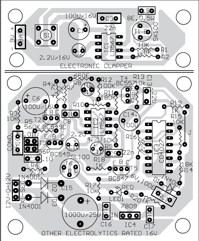
PCB Design: The PCB design for the circuit sound operated on-off switch is shown below.
Figure 6: Solder Side PCB Design of Sound Operated On-off Switch
Figure 7: Component Side PCB design of Sound Operated On-Off Switch
PARTS LIST OF SOUND OPERATED ON-OFF SWITCH
|
Resistors (all ¼-watt, ±5% carbon, unless stated otherwise) |
|
R1, R3, R9, R13, R15, R17 = 10 KΩ R2 = 1.8 KΩ R4 = 4.7 KΩ R5 = 560 KΩ R6, R16 = 2.2 KΩ R7 = 2.7 KΩ R8 = 680 Ω R10 = 1 MΩ R11 = 180 KΩ R12 = 100 KΩ R14 = 18 KΩ R18 – R20 = 1 KΩ |
|
Capacitors |
|
C1, C6, C14 = 100 µF/16V (Electrolytic Capacitor) C2, C10 = 2.2 µF/16V (Electrolytic Capacitor) C3, C9 = 22 nF (Ceramic Disc Capacitor) C4 = 0.01 µF (Ceramic Disc Capacitor) C5 = 56 pF (Ceramic Disc Capacitor) C7, C8, C16, C17 = 0.1 µF (Ceramic Disc Capacitor) C11 = 4.7 µF/16V (Electrolytic Capacitor) C12 = 1 µF/16V (Electrolytic Capacitor) C13 = 0.22 µF (Ceramic Disc Capacitor) C15 = 1000 µF/25V (Electrolytic Capacitor) |
|
Semiconductors |
|
IC1, IC2 = LM567 (PLL tone decoder) IC3 = CD4027 (Dual JK flip-flop) IC4 = 7809 (+9V regulator) T1 = SK100 (PNP medium power transistor) T2, T3 = BC549C (NPN signal transistor) T4 = BC557 (PNP signal transistor) T5 = BC547 (NPN signal transistor) T6 = SL100 (NPN medium power transistor) D1 – D3 = 1N4001 (rectifier diode) LED1 = RED LED |
|
Miscellaneous |
|
RL1 = 9V, 1C/O relay SW1 = Push-to-on tactile switch LS1 = 8Ω, 0.5W loudspeaker B1 = 9V battery MIC1 = Condenser Microphone |


