In this article we see complete details about Schmitt Trigger Buffer IC. We will also see key parameters and its application.
Description of Schmitt Trigger Buffer or Inverter IC | SN7414
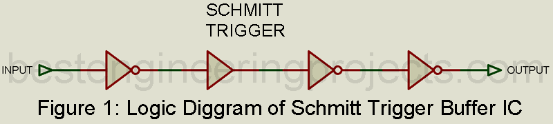
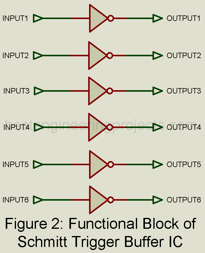
This IC, containing six identical circuits, provides the Schmitt Trigger function and acts as buffer or inverter, as illustrated in the logic diagram if Figure 1. It is particular useful where slowly changing waveforms, such as sine waves, must be squared up, or where noise immunity must be improved. The Schmitt-Triggered circuit conducts over only a narrow “window,” a portion of the total supply voltage. When the input signal is below this hysteresis voltage, nothing passes between input and output.
When the input signal reaches the bottom portion of the hysteresis voltage, the Schmitt Trigger circuit goes into saturation, and when the upper level of the hysteresis voltage is reached, the circuit is cut off. The input signal is changed into a pulse that has the voltage level of the particular logic family. In all other respects the Schmitt-Trigger inverter buffer functions like all other inverter buffer circuits.
Key Parameters of Schmitt Trigger IC
The electrical characteristics are the same as those for the particular digital IC family.
- Quiescent current: The current drawn by the entire IC when no operations are performed. For low-power CMOS devices, 0.5nA and 5V is typical. For high voltage CMOS devices, 0.02 mA is typical up to 15V.
- Hysteresis voltage: The voltage range over which the Schmitt Trigger fires. 0.55 V is typical for low power CMOS with a 5V power supply. For high-voltage CMOS devices 0.9 V is typical for a 5V power supply.
- Threshold voltage: The actual positive and negative voltage that causes the Schmitt Trigger circuit to file and to turn off. For low power CMOS devices, 2.7V is a typical positive going and 2.1V is a typical negative going threshold voltage.
- Propagation delay time: The time required between the arrival of the input signal and the availability of the output signal. For low power CMOS 125 ns is typical and for high voltage CMOS devices 140 ns is typical, both at 5V power supply voltage.
Applications
Schmitt Trigger Buffer or Inverters are used in wave and pulse shapers, as monostable and as astable multivibrators. They are also widely used as receiving circuits in digital transmission systems because the Schmitt-Trigger action greatly improves noise immunity.
Representative Part Number: Texas Instruments SN7414