In this article, we will discuss Multiplexer IC interfacing and different type of multiplexers like Quad 2-input Multiplexer, Dual 4-input Multiplexer, and 8-input multiplexer. We will also show you how to interface with 8-channel multiplexer IC CD4051.
Quad 2-Input Multiplexer | Multiplexer IC Interfacing | CD4051
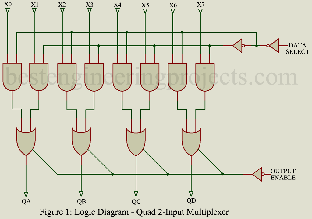
Description: One of the most widely used digital multiplexer configurations is the quad, 2 -input version illustration in figure 1. This particular IC is non-inverting and consists of eight AND and four OR circuits, arranged so that two sets of 4-bit inputs can be selected by the data select signal. As shown in Figure 1 each of the Q outputs is, in effect, a tri-state OR circuit controlled by the output enable signal. This means that any of the Q terminals can be either 0, 1, or a high impedance.
Other digital multiplexer ICs are available that inverts the input, with or without tri-state outputs.
Key Parameters
- Power dissipation: Typical power dissipation during operation is 150 to 250 mW for standard TTL and 15 to 24 mW for low power TTL ICs.
- Propagation delay time: Time required from data input to output. 8 to 10 ns is typical for standard TTL ICs and 40 to 60 ns for low-power TTL ICs.
Applications
The principles of time-division multiplexing in any digital system can be implemented by using multiplexer ICs. A quad 2-input multiplexer can also be used to generate functions of two variables and is useful for multiplexing dual data buses.
Representative Part Number: Signetics 74157.
Comments
Quad 2-input multiplexers are also available with FF storage. The combination of multiplexing with flip-flop (FF) latches is particularly useful in the input/output (I/O) ports of digital computer systems.
A variety of different multiplexer configurations is available in each of the digital IC families.
Dual 4-INPUT Multiplexer | Multiplexer IC Interfacing | CD4051
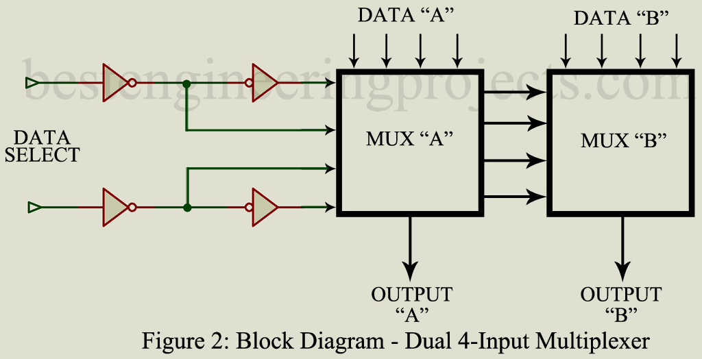
Description: This IC consists of an array of logic gates capable of multiplexing eight data lines into two. As illustrated in the function block diagram of figure 2, the data lines are arranged in groups of four, data A and data B. Each of the two multiplexers (MUX) receives the same four data select signals, derived from two data select inputs. The binary equivalent of the two inputs and their four possible states selects one of the four input lines in each multiplexer and permits one of them to appear at the output. If data group A alternates with data group B outputs, A and B will alternate at the same rate.
The dual 4-input multiplexer is available with inverting or non-inverting features, tri-state outputs, and storage latches.
Key Parameters
- Power dissipation: Typical power dissipation is 170 mW for standard TTL ICs and 31 mW for low-power TTL ICs.
- Quiescent current: The current used by the IC when no operations take place. 5.0 nA at 5 V is typical for low-power CMOS.
- Propagation time delay, data input to output: Time required from data input to output. 200 ns is typical at 5V for low power CMOS, 11 ns is typical for standard TTL, and 14 ns is typical for low-power TTL. ECL ICs have a 4.5 ns propagation delay time.
- Propagation delay time, data selection: The time required from the data selection input until the output changes. 225 ns at 5V is typical for low-power CMOS, 20 ns for standard TTL, and 22 ns for low-power TTL. ECL ICs require only 6.0 ns.
Applications
Whenever time division multiplex is used to combine digital data. This IC can also perform parallel-to-serial conversion and can be cascade in other digital multiplexing configurations.
Representative Part Number: Signetics 74153
Comments
All type of multiplexers is available in every major digital IC family.
8-input Multiplexer | Multiplexer IC Interfacing | CD4051
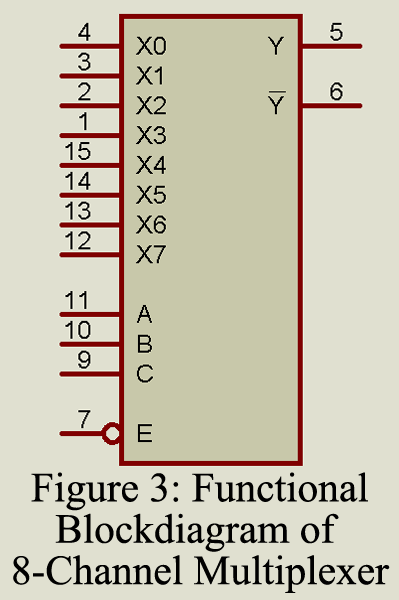
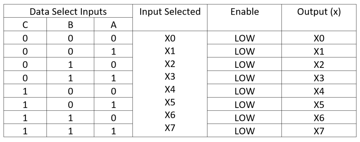
Description: In this IC, one out of eight data inputs is selected for output at the Q and terminal. Three “data select” lines provide the binary input which can have up to eight different values. As illustrated in the function block of figure 3, there is also an enable signal which controls the tri-state output. The truth table of the same illustration shows that, when the enable signal is 1, the Q output will be a high impedance. The data selection by inputs A, B, and C can take place only when the enable signal is 0.
8-input multiplexers are available with temporary storage and without the tri-state output. In the TTL IC family, there are also dual 8-input ICs, using a 24-pin DIP package to provide a selection of one of the 16 data inputs.
Key Parameters
- Power dissipation: Typical power dissipation for the entire IC is 150 to 200 mW for standard TTL ICs, 30 mW for low-power TTL, and 300 mW for low-power CMOS ICs.
- Quiescent current: The total current drawn by the IC when no operation takes place. 5.0 nA at 5V is typical for low-power CMOS, 50 nA is typical for TTL, and 15 nA is typical for low-power TTL ICs.
- Propagation delay time, data input to output: the time required when the data selection is completed until data appear at the output. 10 ns is typical for TTL ICs, 12 to 14 ns is typical for low-power TTL ICs, and 300 ns is typical for low-power CMOS at 5V.
Applications
8-input multiplexers are used whenever digital time division multiplexing methods are applied. These ICs can also be used in data routing, parallel-to-serial conversion, signal gating, number sequence generation, and as part of a Boolean function generator.
Representative Part Number: Texas Instruments SN74151
| A | B | C | E | Q |
| X | X | X | 1 | Hi |
| 0 | 0 | 0 | 0 | D0 |
| 1 | 0 | 0 | 0 | D1 |
| 0 | 1 | 0 | 0 | D2 |
| 1 | 1 | 0 | 0 | D3 |
| 0 | 0 | 1 | 0 | D4 |
| 1 | 0 | 1 | 0 | D5 |
| 0 | 1 | 1 | 0 | D6 |
| 1 | 1 | 1 | 0 | D7 |
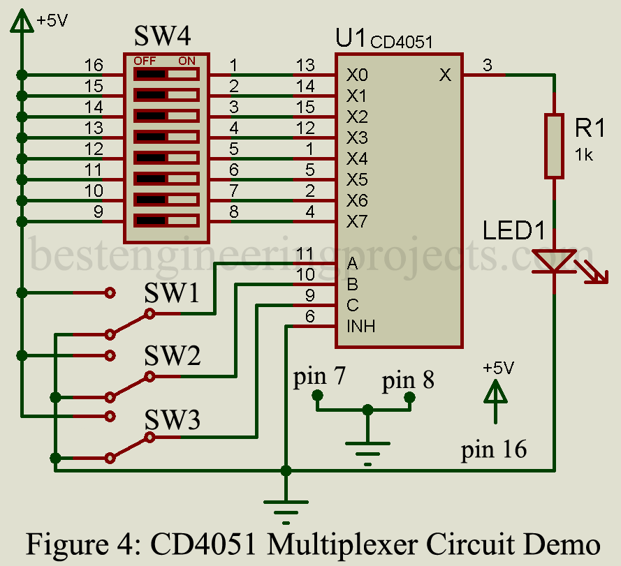
How to interface 8-Input Multiplexer CD4051
