Most of us hear about the variable power supply, it is a power supply unit that provides almost all standard power supplies. How’s that if we combine a variable power supply and a digital control technology. Here, we have designed and verified a DC power supply circuit with the facility of digital control. The unit digital power supply circuit provides a variable, fluctuation-free and regulated ten different DC power supplies. These are 1.5V, 3V, 4.5V, 5V, 6V, 7.5V, 9V, 10.5V, 12V positive power supply, and 12V negative power supply. One can change the output digitally with a push-button switch.
Description of Digital Power Supply Circuit
The digital power supply circuit comprises an adjustable 3-terminal positive voltage regulator IC (LM317), decade counter IC (CD4017), timer IC (NE555), and a fixed negative voltage regulator (LM7912). This circuit is divided into three main sections

Figure: Author Prototype
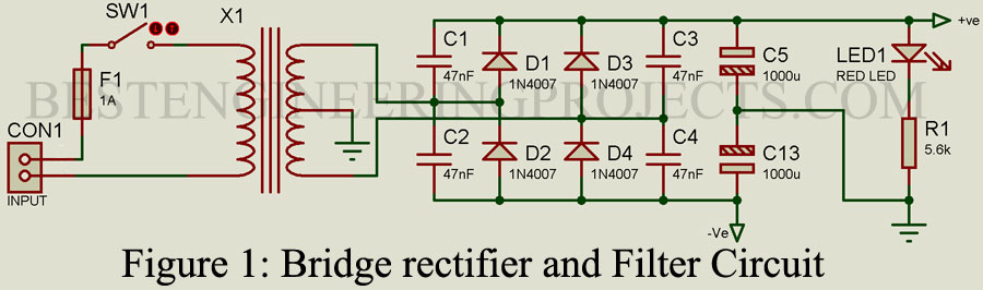
Bridge Rectifier and filter unit:
The input AC of 220V is stepped down by using a center tap 9V-0-9V, 1A secondary transformer. The step-down voltage is rectified using a bridge rectifier built using four diodes D1 through D4. Four ceramic capacitors are connected across four rectifier diodes to bypass undesired spikes and provide smooth and function-free power. Two 1000uF capacitors are connected to smoothen the rectified output. The unregulated, filtered, and fluctuation-free positive and negative power supply is obtained.
Regulated Power Supply Unit
Here we used two regulators to regulate the power supply. One fixed negative voltage regulator to provide negative 12V and a variable voltage regulator with which we will produce almost all standard positive DC power supply.
Negative Power supply:
Negative output from the bridge rectifier is connected to the Vin pin of IC3, where the common pin is connected to the ground of the circuit. From Vout, regulated negative 12V is obtained. Two ceramic capacitors C11 and C12 are used to filter the spikes if available. LED 2 is used here to indicate the negative output. Unlike other LEDs anode of the LED2 is connected to the GND pin whereas the cathode is connected to the Vout pin through a current limiting resistor.
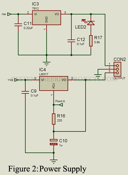
Positive variable power supply:
A positive voltage power supply is built around the variable voltage regulator IC LM317 (IC4). The output voltage obtained is dependent upon the reference voltage between its output and the adjustable terminal. IC4 develops 1.25V normal reference voltage and it appears across resistor R16. The voltage output of IC4 can be calculated by using formula

Here,  and adjustment current IAdj is much smaller in range of microampere which is negligible. Thus the voltage due to this current is neglected. Now, the equation of voltage output becomes

From the above formula, the output voltage can be varied either by varying the value of VRset or by varying the value of R16. Here we are varying the value of the VR set in nine different steps with the help of a digital control unit.
Digital Control Unit
The digital control unit is designed around the timer IC NE555 and decade counter IC CD4017. Timer IC is wired as an astable multivibrator and generates clock pulse when switch SW2 is pressed. Initially, no power supply is available to the timer IC (IC1), when switch SW2 is pressed the timer IC gets a power supply and generates a clock pulse. Whenever this switch is pressed, the timer IC gets a power supply and hence generates a clock pulse. Thus, this switch SW2 is a voltage selector switch. The output clock pulse from pin 3 of IC1 is given to the clock pin of decade counter IC (IC2) through an RC network built using resistor R3 and capacitor C8.
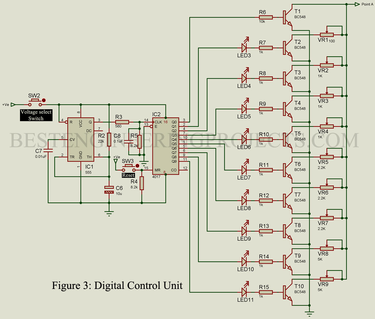
IC2 (CD4017) is a decade ring counter IC i.e. it has 10 outputs ranging from Q0 to Q9. Here we are utilizing all the output to switch ten transistors. Output Q0 of IC2 is connected to the base of transistors T1 through a resistor. This resistor drops the excess voltage and provides only the required voltage to switch the transistor. For the rest of the transistor, this job is done by LED and resistor. As shown in the circuit diagram. This LED is used to indicate the voltage at the output (Refer to table 1). Nine different presets VR1 to VR9 are connected to the collector of transistors T2 to T10 respectively. This preset is used here for voltage adjustment. A push to on switch SW3 is used to reset the decade counter IC (CD4017). When the Reset switch SW3 is pressed all the LEDs (LED3 to LED11) become off.
Table 1
| S.N | Glowing LEDs | Output Voltage |
| 1 | LED3 | 1.5V |
| 2 | LED4 | 3V |
| 3 | LED5 | 4.5V |
| 4 | LED6 | 5V |
| 5 | LED7 | 6V |
| 6 | LED8 | 7.5V |
| 7 | LED9 | 9V |
| 8 | LED10 | 10.5V |
| 9 | LED11 | 12V |
PCB Diagram
PCB of Digital Power Supply Circuit is designed using Altium PCB design software and tools. Solder side and Component side PCB is shown in figure 4 and 5 respectively. Download the actual size solder side and component side from the link given below.
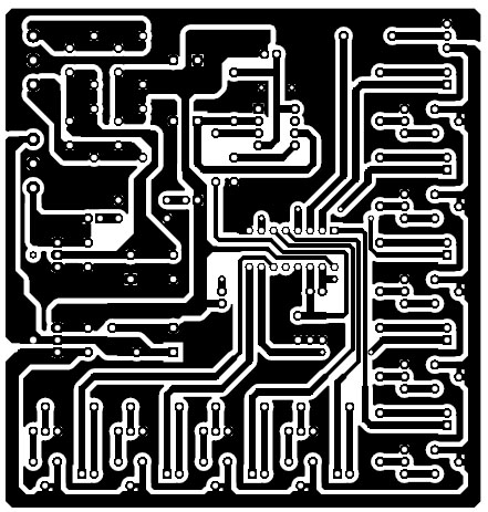
Figure 4: Solder Side PCB
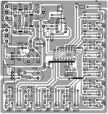
Figure 5: Component side of PCB
Click here to download the PCB
Calibration of Digital Power Supply Circuit:
Now it’s time to calibrate the digital power supply circuit for that, make the PCB, and solder all the components. Connect the transformer secondary terminals to connector CON1.
Step 1: Take a digital multimeter, select DC voltage range and connect its probe to connector CON2.
Step 2: Switch on the power supply and press the reset switch SW3.
Step 3: Press the voltage select switch SW2, and LED3 starts to glow. Adjust VR1 until you get 1.5V.
Step 4: Again press the voltage select switch SW2, and LED4 starts to glow. Adjust VR2 until you get 3V.
Step 5: Follow Step 4 for 4.5V, 5V, 6V, 7.5V, 9V, 10.5V, and 12V.
Step 6: Fix the preset with glue.
Note: Use a proper heat sink for voltage regulator ICs (IC3 and IC4). Since pin configuration these ICs are different so never fix a single heat sink for both ICs.
COMPONENTS LIST REQUIRED FOR DIGITAL POWER SUPPLY CIRCUIT
| Resistor (all ¼-watt, ± 5% Carbon) |
| R1, R7 – R15, R17 = 1 KΩ
R2 = 22 KΩ R3 = 560 Ω R4, R5 = 8.2 KΩ R6 = 10 KΩ R16 = 220 Ω VR1 = 100 Ω VR2 – VR4 = 1 KΩ VR5 – VR7 = 2.2 KΩ VR8, VR9 = 4.7 KΩ |
| Capacitors |
| C1 – C4, C8, C9, C12 = 0.1 µF (Ceramic Capacitors)
C5, C13 = 1000 µF/25V (Electrolytic Capacitors) C6 = 10 µF/25V (Electrolytic Capacitors) C7 = 0.01 µF (Ceramic Capacitors) C10 = 1 µF/25V (Electrolytic Capacitors) C11 = 0.22 µF (Ceramic Capacitors) |
| Semiconductors |
| IC1 = NE555 (Timer IC)
IC2 = CD4017 (Decade Counter IV) IC3 = LM7912 (Negative 12 Voltage regulator) IC4 = LM317 (Positive variable voltage regulator) T1 – T10 = BC548 (General purpose NPN Transistor) D1 – D4 = 1N4007 (Rectifier Diode) |
| Miscellaneous |
| LED1 = RED LED
LED2 = YELLOW LED LED3 – LED11 = GREEN SW1 = ON/OFF Switch SW2, SW3 = Push-to-on Switch F1 = 1A Fuse X1 = 220V AC Primary to 9V – 0 – 9V, 1A Secondary center tap transformer Heat Sink for voltage regulators |
Making video of Digital Power Supply Circuit
I think they are a very nice projects for me . I will start with the battery charger.