Intercoms and calling bells fit properly only in the luxurious hotels, lodges and high class buildings. In small vicinity like small hotels, offices and clinics, these are not the correct options to choose for communication between the working/assisting staffs and people. It is all because of the cost and the fact that this provision can be made for limited number of points and other alternatives are chosen over it i.e. call indication systems.
In early days, such call indications systems employed multiple distinct paths/cables to connect each call point to the indication systems, which produced a complex circuit, challenging installation and particularly for systems with large number of call points involved, this approach was proven more expensive. To avoid complications, a simple and economical room-monitoring system that provides audio-visual identification of the call point has been presented below.
The Distinct Characteristics of the System Call Indicator Using MC68HC705J1A Microcontroller are:
- Uses only two wires for connecting different call points.
- Up to 36 call points (in two circuits comprising 18 call points each) can be connected.
- The control panel has a bright display for visual indication of call point with floor number and a buzzer for audible indication. The buzzer can be snoozed using the Call Acknowledge key.
- The call point number can be changed without changing the wiring.
- The system can be expanded to accommodate more call points in the future.
System Overview of Call Indicator Using MC68HC705J1A Microcontroller
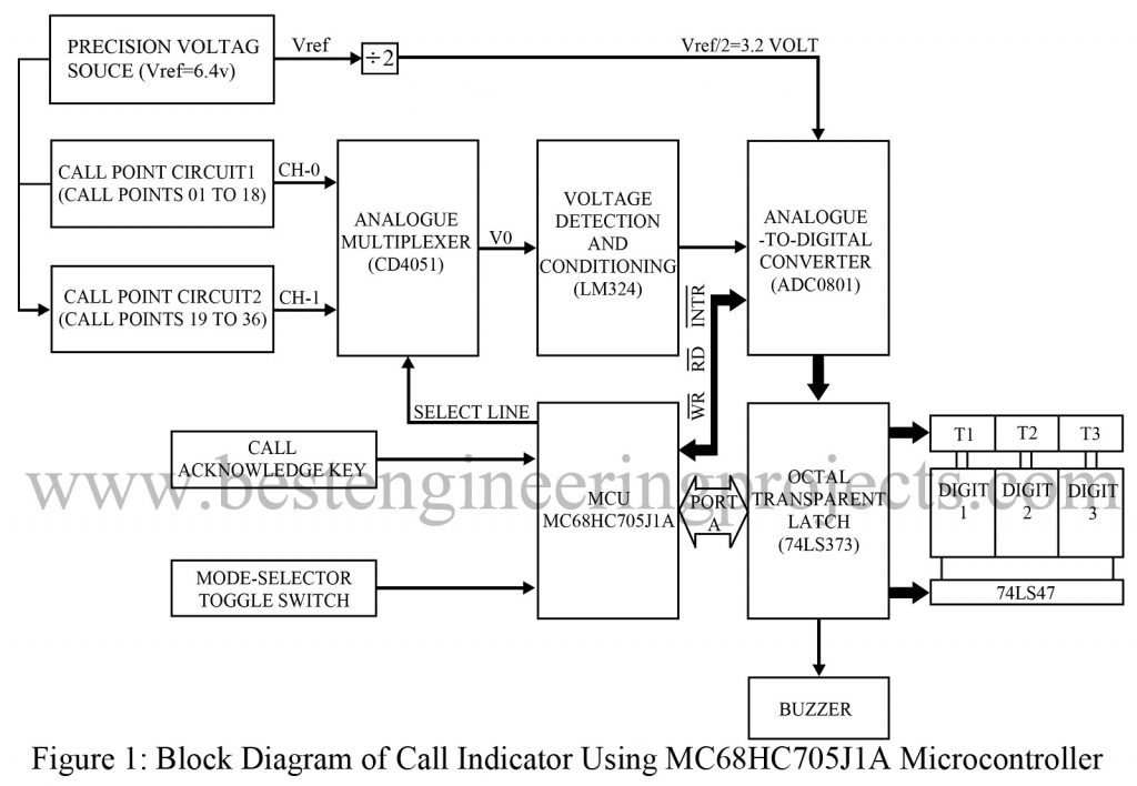
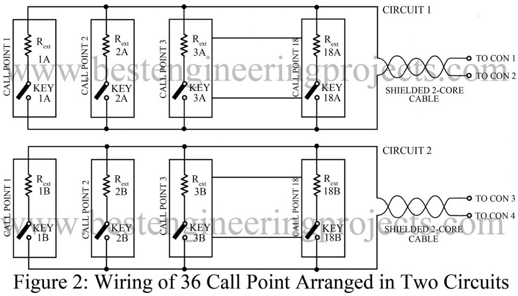
So that the project Call Indicator Using MC68HC705J1A Microcontroller can be easily understood, we have included figures indicating the working of circuit through different dimensions. The first figure, fig, 1 demonstrates the actual block diagram of the Call Indicator Using MC68HC705J1A Microcontroller system, which constitute pathways of connecting multiple call points to a control panel. The connection is made via a two-core shielded cable. To avoid complexity, we have made two distinct circuits to place the call points. This concept is proven to be of much help when call points are located on different floors. A single circuit can connect 18 call points. Hence, the entire system can withstand 36 distinct set of call points.
And, the second figure, fig.2 illustrates how different call points are located within the two-circuit frame. You can go through table 1 to find compatible connection settings for different call point numbers, be it on the same floor or on different floors.
TABLE 1 | Call Indicator Using MC68HC705J1A Microcontroller
| Distribution of call point | Suggested Mode | Call Point Connection Details | Numbering of Call Point |
| 18 or more call point on the same floor | 0 | Connect call point circuit-1 output to CON1 and CON2 | 001 to 036 |
| Connect call point circuit-2 output to CON3 and CON4 | |||
| 18 or less call points only 1st floor | 1 | Connect call point circuit-1 output to CON1 to CON2 | 001 to 018 |
| CON3 and CON4 unused | |||
| 18 or less call points on two floors | 1 | Connect call point circuit-1 output to CON1 and CON2 | 001 to 018 |
| Connect call point circuit-1 output to CON1 and CON2 | 101 to 118 |
The hardware | Call Indicator Using MC68HC705J1A Microcontroller
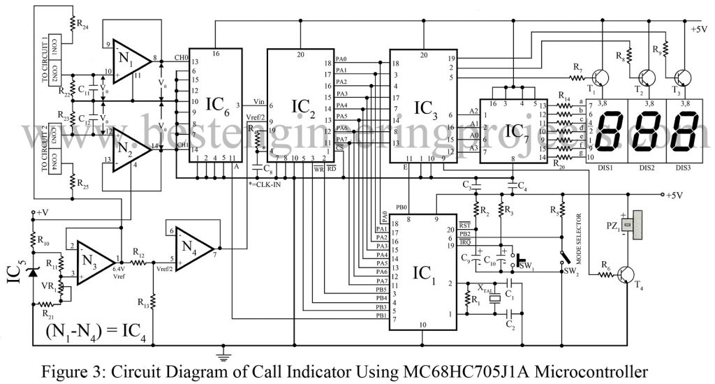
The core component of the project Call Indicator Using MC68HC705J1A Microcontroller is Motorola’s MC68HC705J1A microcontroller. The detailed hardware connection of this project is given by the figure 3. According to the functions each portion carries, this section can be further branched into four typical parts: namely, call-point detection section, analogue-to-digital conversion (ADC) section, display section and microcontroller section.
The overall operation can be explained as below:
- Call-point detection section- identifies if a key is pressed from call point
- ADC section- converts the fixed DC voltage which is defined by the resistor connected in series with key, into the equivalent digital data.
- Microcontroller section- decodes the information form ADC.
- Display section- displays the call point number once data is decoded by the microcontroller.
The call-point detection section | Call Indicator Using MC68HC705J1A Microcontroller
As stated earlier, we have used two-core shielded cable to establish both internal as well as external connection of the call points to the control unit. The reason why we chose shielded cable is for its resistance to noise that somehow reduces the noise in the overall system. In the figure 2, series resistors connected with corresponding keys; 1 to 18 are indicated by Rext-1 to Rext-18 . Same values of resistors are used in both call point circuits.
The supply for call-point circuits 1 and 2 is provided by a 6.4V reference source which is a fixed and temperature-compensated source. In order to limit the current drawn from the source, resistors; R24 and R25 (each of 1.2k) are applied. The circuit board includes two fixed resistors: R22 and R23, two capacitors; C11 and C12 (each of 0.1 uF) that bypass the noise signals. When any key is pressed, there is voltage drop across internal resistors R22 and R23, which is denoted by V0. Table II comprises voltage drop values for each key, corresponding to the set of value of external resistor and call point number. Here in the circuit, the drop voltage value V0 is defined by the series resistor connected along with key, once the key has been pressed. The voltage thus generated is then forwarded through the two-core shielded cable.
TABLE 2 | Call Indicator Using MC68HC705J1A Microcontroller
| Rext | V0 = 64*10k
(11.2k+Rext) |
ADC Equi D=V0 25*10-3 | Range of Identification | Call Point Number |
| 220k (Rext-1) | 64/231.2=0.2768 | 11 | 07-15 | 01 |
| 100k (Rext-2) | 64/111.2=0.5755 | 23 | 16-26 | 02 |
| 68k (Rext-3) | 64/79.2=0.808 | 33 | 27-38 | 03 |
| 47k (Rext-4) | 64/58.2=1.0996 | 44 | 39-50 | 04 |
| 33k (Rext-5) | 64/44.2=1.4479 | 58 | 51-62 | 05 |
| 27k (Rext-6) | 64/38.2=1.6753 | 67 | 63-72 | 06 |
| 22k (Rext-7) | 64/33.2=1.9277 | 77 | 73-82 | 07 |
| 18k (Rext-8) | 64/29.2=2.1917 | 88 | 83-92 | 08 |
| 15k (Rext-9) | 64/26.2=2.4427 | 98 | 93-103 | 09 |
| 12k (Rext-10) | 64/23.2=2.7586 | 110 | 104-114 | 10 |
| 10k (Rext-11) | 64/21.2=3.0188 | 120 | 115-125 | 11 |
| 8.2k (Rext-12) | 64/19.4=3.2989 | 132 | 126-137 | 12 |
| 6.8k (Rext-13) | 64/18=3.5555 | 142 | 138-147 | 13 |
| 5.6k (Rext-14) | 64/16.8=3.8009 | 152 | 148-156 | 14 |
| 4.7k (Rext-15) | 64/15.9=4.0251 | 161 | 157-170 | 15 |
| 3k (Rext-16) | 64/14.2=4.5070 | 180 | 171-188 | 16 |
| 2k (Rext-17) | 64/13.2=4.8484 | 194 | 189-200 | 17 |
| 1k (Rext-18) | 64/12.2=5.2459 | 210 | 200 and above | 18 |
This project employs one extra component; CMOS analogue multiplexer CD4051 (IC6) which is a single 8-channel multiplexer and has binary control inputs; A, B and C. These three binary signals chose one channel from the eight channels and then connect it to the output following the details provided in fig.3. However, here we have implemented only two of its channels to serve our purpose.
The call-point1output is connected to channel-0(CH-0) and call-point2 output is connected to channel-1(CH-1). The outputs of two circuits are simultaneously scanned with the help of a multiplexer.
Voltage is critical parameter in our circuit, since little change in reference voltage Vref can cause the change in voltage drop V0 which gradually leads to false identification of the call-point number and the project fails. Therefore, Vref must be a fixed and temperature-compensated voltage source. Vref is derived from National Semiconductor’s active temperature-compensated reference zener diode LM329 (IC5). This IC has a very low dynamic impedance of 0.8ohm impedance which minimizes the errors due to input voltage variations, load variations and feed resistor drift. It offers a fixed output voltage of 6.9V. In initial conditions, voltage V0 is set to zero. When a key is pressed, the value of V0 is calculated as:
V0 = Vref * (R22)/(R24 + Rext + R22) Volts
Where R24 is 1.2 kilo-ohms and R22 is 10 kilo-ohms.
Another IC LM324 is employed in the circuit that comprises N1 through N4 (IC4) and is used as a voltage follower to shield the respective voltage signals.
The ADC section | Call Indicator Using MC68HC705J1A Microcontroller
The ADC portion receives the analogue value of potential drop developed across resistor R22 once the key is pressed. From the table II, we can conclude the drop voltage ranges from 0 volt to 5.25 volts. Here, IC ADC0801 (IC2) converts this value into respective digital equivalent.
The ADC IC2 is an 8-bit, successive approximation-type, CMOS analogue to-digital converter fabricated in a 20-pin dip package. It operates on a low supply voltage (0 to 5 volts) and a single power supply (5 volts). Two separate input pins are adjusted in this IC namely, Vin (+) pin and V (-) pin, for the differential analogue signal. In cases when the analogue signal is single ended and positive, i.e. it varies from 0 volt to 5 volts, Vin (+) pin is used as the input and V(–) pin is grounded.
The clock required for the converter is provided via pin-4, the frequency of which can vary from 100 kHz to 800 kHz. The clock can be provided both internally and externally. A set of resistor and capacitor connected externally at pins 19 and 4 form the built-in internal clock. Else, one can also connect an external clock at the CLK-IN pin of IC to provide external clock for IC. We opted out for the second choice, the value of frequency is determined by:
For interfacing purpose, three control signals of IC2 (CS, WR and RD) are implemented. For low state of chip-select (CS) pin, IC2 is enabled. The low state of WR pin resets the internal successive approximation register (SAR) and causes the output lines go to high-impedance state. For state change of WR pin from low to high, the conversion begins.
Once the conversion process completes, the interrupt request pin INTR is declared low and then the data is placed on the output lines. The low state of read pin (RD) ensures the data has been read and the interrupt pin (INTR) gets reset.
For a supply (Vcc) of 5 volts, the input voltage varies from 0 to 5 volts and output range for this input is 00H to FFH. At times, we can limit high level outputs for low level inputs by using a Vref/2 pin. The value of voltage defined at this point decides the step size of conversion.
It is found after taking account of voltage level at Vin (+) pin, that the most appropriate step size for ADC is calculated to be 25 mV (6.4/256 = 25 mV). Therefore, we arrive at conclusion; ADC transforms an analogue voltage signal of 6.4 volts from pin Vin (+) into FFH (11111111b) at the output data pins. To obtain a conversion period of about 100 µsec, the clock frequency of ADC is set roughly 600 kHz.
As designated, ADC constantly converts information/data from analogue source into digital form. As a result, hazardous situations of system failure and malfunctioning caused by pressing large number of infinite keys at a time. can be avoided.
Different values of analogue voltage V0 and their corresponding digital equivalent values for different call point numbers are included in Table II. Initially, when no keys are pressed, V0 is equal to 0 volts and its digital equivalent output from ADC is 00D. When key is pressed, digital output ranges from 10D to 200 D as illustrated by the table II. The microcontroller performs remaining work of presenting this digital data into useful call point number.
The latch and display section | Call Indicator Using MC68HC705J1A Microcontroller
Here comes the most important part of all that includes display device which is a crucial part to establish proper connection between the user and the machine. Here we have selected three 7-segment displays (DIS1 through DIS2 for displaying the call point information. These devices are driven using the time-multiplexed technique. The three displays (DIS1 through DIS3 displays the floor number, and call point numbers accordingly.
Same input lines are used by these 7-segment displays which is a common thing about them. Whatever digit is entered in the first attempt, it enables the first display segment out of other 7-segment display units used in the circuit. However, the data fed as the first digit gets sooner replaced by the second digit and the second display is enabled. Following the same pattern, all digits are displayed on the display units accordingly. This process repeats itself. Since the repetition follows 100 times in a second, some sort of illusion of digits being continuously displayed appears. In order to assist driving the common-anode displays, BCD-to-7-segment decoder/ driver 74LS47 (IC7) and 2N2907 (T1 through T3) are employed.
Talking about microcontroller (IC1), both reading output obtained from ADC as well as displaying data is done via Port A. Problems of bus contention may arise leading to circuit interruption. To avoid this, an octal transparent latch 74LS373 (IC3) is used. During refreshing the digital displays, latch becomes transparent and then one by one, digits of concerned data are displayed. For RD and WR lines are high in this scenario, data lines of ADC0801 are in high-impedance state. When the refreshing process stops, the latch is made non-transparent. Further changes in data line of ADC won’t impose changes on data displayed on the screen.
For instance, 126 be the data to be displayed, the BCD equivalent of which (0001) is placed on the input lines of IC 74LS47 (IC7). The output of IC 74LS47 provides the 7-segment equivalent data of 01. Through the help of transistor T1, the first digit, digit-1 is chosen. And, the digit is displayed on DIS1 for approximately 2 milliseconds. Following same pattern, digit-2 and 3 are displayed on DIS2 and DIS3 for an interval of 2 ms each through the help of transistors T2 and T3. The duration of interrupt generation for the timer interrupt is in every 10 ms. It is the duration during which all the displays used in the project are refreshed.
The microcontroller section | Call Indicator Using MC68HC705J1A Microcontroller
The project employs microcontroller as one of its core component. Here, Motorola’s MC68HC705.J1A microcontroller (IC1) is programmed such that it offers multiple functions:
- Continuously scan the keys to identify pressing of any key
- Read the data obtained from ADCO801
- Identify the destination where key is pressed
- Display the call point number and also provide audio indication
- Check for the pressing of Acknowledge key to snooze the buzzer
The connection setting for microcontroller is clearly shown in Fig. 3. As stated earlier, port A is used for reading the ADC data as well as the display data. Only difference is that while reading ADC data, it is configured in input mode and for data display, it is configured in output mode. Port B is used as the control port. It performs controlling functions for both the ADC and the latch.
Power supply | Call Indicator Using MC68HC705J1A Microcontroller
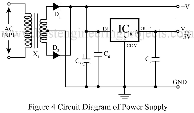
The section that provides fuel to the circuit is power supply part, the clear picture of which is depicted by the fig.4. The circuit requires a secondary output of 12V-0-12V AC, 300mA for this a step down transformer X1 is used. Thus generated transformer output is rectified by a full-wave rectifier that constitutes diodes D1 and D2 and later filtered by capacitor C5. The direct +V output from the supply circuit is used for IC LM324 (IC4) and the reference circuit, while the regulated 5V from regulator IC 7805 (IC8) is used to power the entire circuit excluding IC4 and the reference circuit.
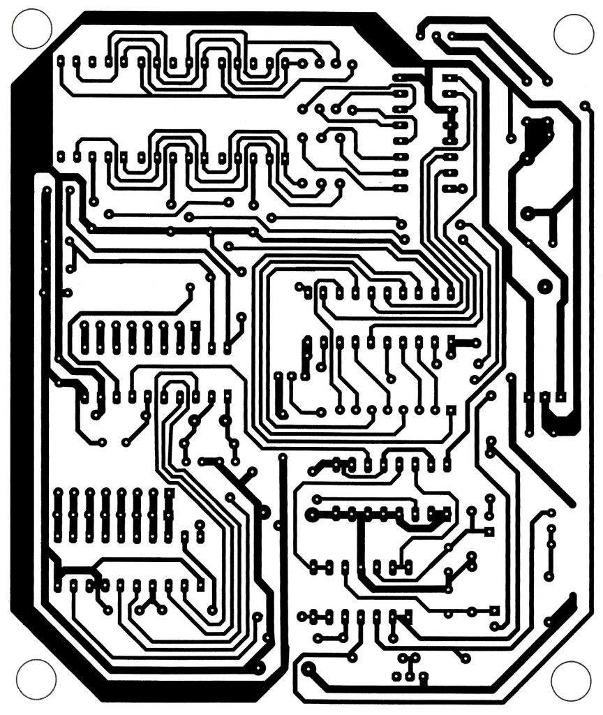
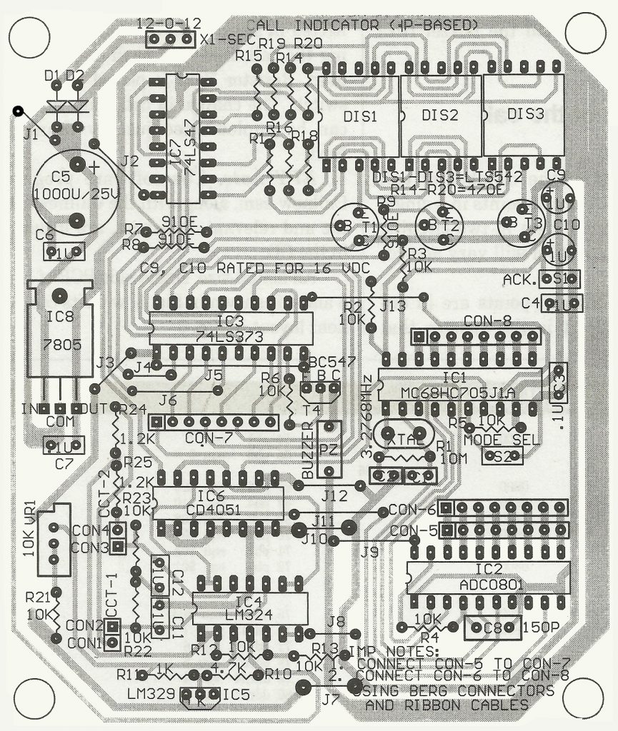
Fig.5 illustrates the single side of actual sized PCB for fig. 3 and 4 and Fig.6 shows the component layout.
Figure 4: Actual Size Solder Side PCB
Figure 5: Actual Size Component Side PCB
PARTS LIST OF CALL INDICATOR USING MC68HC705J1A MICROCONTROLLER
| Resistor (all ¼-watt, ± 5% Carbon) |
| R1 = 10 MΩ
R2-R6, R12, R13 = 10 KΩ R7 – R9 = 910 Ω R10 = 4.7 KΩ R11 = 1 KΩ R14 – R20 = 47 Ω R21 = 18 KΩ R22, R23 = 10 KΩ R24, R25 = 1.2 KΩ |
| Capacitors |
| C1 – C4, C6, C7 = 27 pF (Ceramic Disc)
C5 = 1000 µF, 25V (Electrolytic Capacitor) C8 = 150 pF (Ceramic Disc) C9, C10 =1 µF, 16V (Electrolytic Capacitor) C11, C12 = 0.1 µF (Ceramic Disc) |
| Semiconductors |
| IC1 = MC68HC705J1A (microcontroller)
IC2 = ADC0801 (8-bit analog to digital converter) IC3 = 74LS373 (octal transparent latch) IC4 = LM324 (quad operational amplifier) IC5 = LM329 (temperature compensate ref. diode) IC6 = CD4051 (analogue multiplexer) IC7 = 74LS47 (BCD-to-7-segment decoder/driver) IC8 = 7805 (+5V regulator) T1 – T3 = 2N2907 (NPN transistor) T4 = BC547 (NPN transistor) D1, D2 = 1N4007 (rectifier diode) DIS1 – DIS3 = LST542 (7-segment common anode display) |
| Miscellaneous |
| X1 = 230V Primary to 12V-0-12V, 300 mA secondary transformer
XTAL1 = 3.2768MHz crystal PZ1 = Piezo buzzer SW1, SW2 = Push-to-on switch |
The software | Call Indicator Using MC68HC705J1A Microcontroller
The suitable software offered by the Motorola for the purpose of programming and development of overall system is integrated development environment (IDE). The editor, assembler and programmer software that comes along with development tool offer extra support for the Motorola’s device programmer and a software simulator. The ICS05JW in-circuit simulator, along with the development board (pod), forms a complete simulator and non-real-time input/output emulator for simulating, programming and debugging the code of an MC68HC705J family device.
During the simulation of the code, as you connect the pod as an interfacing media between your host computer and target hardware, we can use the actual inputs and outputs of the target system ISC05JW software can also be used in order to edit and assemble the code in standalone mode, without input/output to/from the pod. The fact that the pod (MC68HC705J1CS) can be interfaced to any IBM computer running on Windows 3.X/Windows 9X using the serial port increases the system flexibility.
The following functions are performed by the software program:
- Initialize ports A and B, timer and display
- Monitor pressing of keys using the ADC
- Display the data
- Identify the call point number
Considering facts like simplicity of the program, easy debugging and precise functioning of the system, multiple data manipulation tricks and internal branching techniques are must. And, therefore, the software is further sectioned into Initialize, Identify, DispCon, Refresh, Read and Acknowledge modules. IT makes us easy to understand the sequence of operation and programming logic. A brief description of each module is given below.
Init- During this module, microcontroller ports are assigned. Firstly, ports A and B are assigned as the output ports. During that, the latch is made transparent and since no key is pressed, 000 is shown by the display. The timer interrupt is initialized to give an interrupt every 10 ms.
Identify- In this section, data obtained from the ADC data is analyzed and the corresponding call point destination is identified. If any key is found pressed, the particular call point number is stored in hex form in the display register.
CLICK HERE TO DOWNLOAD SOURCE CODE
Interesting